
Kernullist’s article is a deep defensive walkthrough of external PCIe DMA cheats, a class of game-cheating hardware that avoids traditional anti-cheat scanning because no cheat code runs on the gaming PC. The setup usually includes a second “cheat PC,” an FPGA-based PCIe endpoint installed through an M.2 or PCIe slot, and sometimes a USB HID actuator for mouse or keyboard input. The DMA card uses bus-mastering to issue PCIe memory-read transactions against the target machine’s RAM, while anti-cheat software sees only a seemingly normal PCIe device. The article explains why detection must move below user-mode and kernel-mode telemetry into PCIe configuration space, TLP behavior, link-state fingerprints, IOMMU policy, ACS topology, ATS/PASID trust, AER errors, TPM-backed measured boot, VBS/HVCI, and external attestation. It also distinguishes weak public PCILeech-style firmware from more advanced 1:1 configuration-space emulation. The key takeaway is that no single signature is durable: realistic defense requires layered verification of hardware identity, DMA isolation, firmware state, and runtime behavior.
External DMA cheats are the hardest game-cheating threat to defend against, because the cheat code does not live on the machine running the game. The “victim” PC sees only a passive-looking PCIe endpoint while a second PC, connected to that endpoint, reads game state at line rate and feeds it into an aimbot or wallhack. Conventional anti-cheat techniques — syscall hooks, memory scanners, code-integrity checks — cannot find what is not there. Detection has to move down the stack, into the PCIe protocol itself, into the IOMMU, and ultimately to external trust anchors. This is a technical walk through that stack from a defender’s perspective.
1. Threat Model
A modern external DMA cheat consists of:
- The cheat PC — an ordinary computer running the cheat application, signature databases, aim assistance, ESP rendering, and a network or USB link to the gaming PC.
- The DMA card — an FPGA-based PCIe endpoint installed in the gaming PC (typically in an M.2 NVMe slot). It exposes a memory-read/write interface to the cheat PC and uses its Bus Master capability to issue Memory Read TLPs against the gaming PC’s RAM.
- An optional actuator — a USB HID emulator (often microcontroller-based) that injects keyboard/mouse input on the gaming PC according to commands from the cheat PC, closing the loop. This document focuses on the DMA card and treats the actuator as a peripheral concern.
The structural property that makes the threat distinctive is that no attacker code executes on the gaming PC. Step (2) is a hardware-level transaction between the FPGA and the gaming PC’s memory controller, mediated by the chipset and (when configured) the IOMMU. The gaming PC’s OS, drivers, and any anti-cheat running on it see only a PCIe device announcing itself through Configuration Space and performing what looks like ordinary DMA.
Defense has three layers, each with progressively stronger guarantees but progressively more complex deployment:
| Layer | Mechanism | What It Catches |
|---|---|---|
| PCIe-layer fingerprinting | Inspect Configuration Space and behavior at the bus level | Identity mismatch — spoofed device that doesn’t match a real silicon’s full signature |
| IOMMU enforcement | Use the IOMMU to bound what physical memory the device can touch | Out-of-domain DMA — device trying to read game memory it wasn’t allocated |
| External attestation | TPM-anchored measured boot, cloud-verified | Boot-chain compromise — IOMMU or kernel itself subverted |
The rest of this document explains each layer from first principles, then synthesizes them into a layered detection pipeline.
2. The PCIe Protocol Stack
Almost everything a defender does at the bus level depends on understanding PCIe’s three protocol layers and the Configuration Space mechanism that sits above them.
2.1 The Three Layers
PCIe is a packet-switched, point-to-point serial protocol. Every transaction passes through three layers in both directions:
| Layer | Unit | Function |
|---|---|---|
| Transaction Layer | TLP (Transaction Layer Packet) | Memory/IO/Config reads & writes, completions, messages |
| Data Link Layer | DLLP (Data Link Layer Packet) | Acknowledgements, flow control credits, power management |
| Physical Layer | Ordered Sets, encoded symbols | Link training, equalization, clock recovery |
A real device’s behavior is shaped by all three layers. An FPGA emulating a real device only fully controls the Transaction Layer; the Physical and Data Link layers leak fingerprints that BRAM-based emulation cannot fully hide.
2.2 The Transaction Layer and TLP Format
A TLP is the unit of work in PCIe. Every TLP begins with a 3 DW (12-byte) or 4 DW (16-byte) header; 4 DW headers are used for 64-bit addresses and certain message types. The first DWord encodes the TLP type and routing properties:
| Bits | Field | Notes |
|---|---|---|
[31:29] | Fmt[2:0] | Header format and presence of data (see Fmt encoding below) |
[28:24] | Type[4:0] | TLP type, combined with Fmt |
[23] | R (or T9 in some specs) | Reserved |
[22:20] | TC[2:0] | Traffic Class (default 0) |
[19] | R (or T8) | Reserved |
[18] | Attr[2] | ID-Based Ordering (IDO) |
[17] | LN | Lightweight Notification |
[16] | TH | TLP Processing Hint |
[15] | TD | TLP Digest present (ECRC trailer follows) |
[14] | EP | Poisoned data |
[13:12] | Attr[1:0] | Relaxed Ordering (RO), No Snoop (NS) |
[11:10] | AT[1:0] | Address Type (see below) |
[9:0] | Length[9:0] | Payload length in DWords (0x000 encodes 1024 DW = 4 KB) |
Fmt[2:0] encoding:
Fmt | Meaning |
|---|---|
000 | 3 DW header, no data |
001 | 4 DW header, no data |
010 | 3 DW header, with data |
011 | 4 DW header, with data |
100 | TLP Prefix (precedes another TLP) |
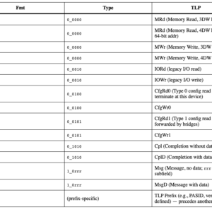
The combination of Fmt[2:0] (format) and Type[4:0] (type) determines what the TLP is:
| Fmt | Type | TLP |
|---|---|---|
000 | 0_0000 | MRd (Memory Read, 3DW header) |
001 | 0_0000 | MRd (Memory Read, 4DW header — 64-bit addr) |
010 | 0_0000 | MWr (Memory Write, 3DW header) |
011 | 0_0000 | MWr (Memory Write, 4DW header) |
000 | 0_0010 | IORd (legacy I/O read) |
010 | 0_0010 | IOWr (legacy I/O write) |
000 | 0_0100 | CfgRd0 (Type 0 config read — terminate at this device) |
010 | 0_0100 | CfgWr0 |
000 | 0_0101 | CfgRd1 (Type 1 config read — forwarded by bridges) |
010 | 0_0101 | CfgWr1 |
000 | 0_1010 | Cpl (Completion without data) |
010 | 0_1010 | CplD (Completion with data) |
001 | 1_0rrr | Msg (Message, no data; rrr = routing subfield) |
011 | 1_0rrr | MsgD (Message with data) |
100 | (prefix-specific) | TLP Prefix (e.g., PASID, vendor-defined) — precedes another TLP |
Other DW0 fields that matter for detection:
TC[2:0]— Traffic Class. Default 0; real silicon rarely uses non-zero TC. A spoofed device generating non-zero TC is anomalous.Attr[2:0]—RO(Relaxed Ordering),NS(No Snoop),IDO(ID-Based Ordering). A device emulating a NIC must follow that NIC’s typical NS/RO usage pattern; mismatches are visible.AT[1:0]— Address Type.00= Untranslated (the IOMMU will translate),01= Translation Request (ATS only),10= Translated (device claims it has already translated via ATS, IOMMU may pass through). This field is the basis of bypass technique #5 in §7.3.TD— TLP Digest. If set, an ECRC trailer is present.EP— Poisoned. Indicates data is known-bad; used in some error scenarios.Length— Payload length in DWords. 0 means 1024 DWs (4 KB).
DW1 carries the Requester ID (16 bits = Bus:Device:Function, “BDF”) and a Tag (8 bits) used to match completions to requests. For Configuration TLPs, DW2 additionally carries the target Bus:Device:Function and Register Number being addressed. For Completions, DW1 carries the Completer ID and a 3-bit Completion Status:
| Status | Meaning |
|---|---|
000 | Successful Completion (SC) |
001 | Unsupported Request (UR) |
010 | Configuration Request Retry Status (CRS) |
100 | Completer Abort (CA) |
The distinction between UR and CA matters for spoofing detection — real silicon responds differently to malformed config accesses than to accesses to unimplemented offsets, and many spoofed firmwares hard-code one or the other.
TLP routing. Three modes exist:
- Address routing — used for Memory and IO TLPs. The TLP’s address field is matched against each bridge’s downstream apertures.
- ID routing — used for Configuration TLPs and Completions. The target BDF (in Cfg) or Completer/Requester ID (in Cpl) selects the path.
- Implicit routing — used for some Messages (e.g., broadcast, terminate at root).
A device’s BDF is its identity for everything that matters: IOMMU translation lookup, ACS source validation, AER source identification, MSI/MSI-X routing. The Requester ID is the entire input to per-device security policy. Anything that lets a device send TLPs with a different Requester ID — broken ACS Source Validation (§5.2), malicious PCIe switch, certain DMA-from-DMA abuses — fundamentally compromises isolation.
Posted, Non-Posted, and Completion categories. Every TLP belongs to one of three transaction categories:
- Posted (P) — fire-and-forget. Memory Writes, Messages. No completion comes back.
- Non-Posted (NP) — requires a completion. Memory Reads, IO Reads/Writes, Configuration Reads/Writes.
- Completion (Cpl/CplD) — the response to a Non-Posted request.
PCIe ordering rules (Base Spec Section 2.4, Transaction Ordering) state, briefly: a Posted request cannot pass an earlier Posted request (preserving write order); a Read Request cannot pass an earlier Posted Request to the same destination (so reads observe prior writes); Completions can pass earlier Posted Requests by default, modulated by RO and IDO attributes. These rules are why completion latency distribution has a characteristic shape — DRAM-backed devices serialize reads against pending writes through the memory controller, while BRAM-backed emulators have no such contention.
Memory Read completions are split. A single Memory Read TLP can return a payload of up to Max_Read_Request_Size (MRRS) bytes — typically 512 or 4096. That payload rarely comes back in a single Completion TLP. The completer is allowed to split it at any boundary ≥ RCB (Read Completion Boundary, advertised in Link Control as 64 or 128 bytes), and each split fragment cannot exceed Max_Payload_Size (MPS). On a typical platform with MPS = 128–512 and RCB = 64, a 4 KB read arrives as anywhere from a handful to several dozen separate CplD TLPs.
Each Completion carries enough information for the requester to reassemble:
Lower Address[6:0]— the lowest 7 bits of the byte address of the first byte of data in this Completion.Byte Count[11:0]— number of bytes still remaining in the read after accounting for everything before this Completion (i.e., the Byte Count of the first fragment equals the total requested size; the last fragment’s Byte Count equals its own payload length). When Byte Count matches the bytes contained in the current Completion, this is the final fragment.BCM(Byte Count Modified) — historical PCI-X compatibility bit; typically 0 in PCIe.Tag— matches the originating MRd’s Tag, identifying which outstanding read this belongs to.
The split pattern (how many fragments, where the boundaries fall) is determined by the completer’s internal pipeline, memory controller arbitration, and concurrent traffic. It is a strong fingerprint: a real memory controller serving a 4 KB read against contended DRAM produces a characteristic distribution of fragment sizes and inter-fragment gaps; a BRAM-backed emulator producing perfectly uniform 64-byte fragments at constant cadence is anomalous.
Tag space limits outstanding reads. Originally PCIe used a 5-bit Tag (32 outstanding non-posted requests per Requester ID). PCIe 1.1+ added an Extended Tag option, enabled at Device Control [8], that extends the field to 8 bits (256 outstanding). PCIe 4.0+ added 10-Bit Tag, enabled separately at Device Control 2 [12], that extends further to 10 bits (1024 outstanding). On modern systems Extended Tag is typically enabled by default in firmware. Tag turnover discipline — the pattern of which tags get reissued and how quickly — reflects the device’s internal request tracking pipeline. Firmware that issues reads with no tag turnover at all (every read carries the same tag, or tags increase monotonically beyond the negotiated implementation limit) is observably distinct from real silicon.
MPS and MRRS as fingerprints. Both are negotiated once at link bring-up and fixed for the session. Device Capabilities [2:0] advertises Max_Payload_Size_Supported (encoding: 0=128, 1=256, 2=512, 3=1024, 4=2048, 5=4096 bytes); Device Control [7:5] carries the current MPS, which must be ≤ Supported and is set by the OS to the minimum of all devices in the hierarchy. Device Control [14:12] is Max_Read_Request_Size (same encoding). Do not overstate this as an Artix-7-only ceiling: AMD/Xilinx PG054 documents 7-series integrated-block advertised MPS values of 128, 256, 512, or 1024 bytes, with 1024 not supported for the 8-lane, 5.0 GT/s, 128-bit core configuration. MPS/MRRS are still useful fingerprints, but the discriminator is donor consistency: a device claiming a donor that is known to support larger payloads, different tag behavior, or a different negotiated profile should match that donor under the same root-port constraints.
2.3 The Data Link Layer
DLLPs sit between the Physical and Transaction Layers and provide reliable delivery. The major DLLP types:
| DLLP | Purpose |
|---|---|
Ack | TLP received correctly |
Nak | TLP received with error; sender must replay |
InitFC1 / InitFC2 | Flow Control credit initialization at link bring-up |
UpdateFC | Ongoing flow control credit updates |
PM_* | Power management requests/acknowledgements (L0s, L1 entry/exit) |
Vendor | Vendor-defined DLLPs |
Every TLP carries a 12-bit Sequence Number. The receiver acknowledges via Ack DLLPs; the sender keeps each TLP in a Replay Buffer until acknowledged, retransmitting on Nak or timeout. Where root-port performance counters expose replay-related metrics, the signal is comparative: a session whose replay/recovery rate departs materially from a reference baseline for the donor under the same platform conditions is anomalous, regardless of absolute magnitude.
Flow control credits are advertised separately for each TLP category and for header vs payload:
| Credit Type | What It Covers |
|---|---|
PH / PD | Posted Header / Posted Data |
NPH / NPD | Non-Posted Header / Data |
CplH / CplD | Completion Header / Data |
A device must not transmit a TLP unless its receiver has advertised enough credit. Modern PCIe IP cores handle credit accounting automatically. The important operational correction is that these negotiated credit values are notgenerally exposed through the standard Link Capabilities register. They are visible in protocol-level traces, in some root-port/vendor performance counters, or from FPGA-side debug instrumentation. Therefore, flow-control credit shape is useful for lab fingerprinting and high-value forensic captures, but it should not be listed as a normal runtime config-space detector.
2.4 The Physical Layer
Two physical-layer details matter to a defender even without access to PHY-level instrumentation.
LTSSM (Link Training and Status State Machine). Every PCIe link has its own LTSSM, traversing states from Detect through Polling, Configuration, L0 (operational), and possibly L0s, L1, L2 (low-power), Recovery (after signal issues), Hot Reset, Disabled, and Loopback. The current state is visible via the Link Status Register (covered in §3.3) and root-port performance counters. Detection-relevant observations:
- Negotiated Link Width (
Link Status[9:4]). A device advertising x16 capability but negotiating x1 is a tell — particularly if its donor model is a GPU that should always negotiate higher widths in a typical slot. - Current Link Speed (
Link Status[3:0]). A device whose capability claims Gen4 but stays at Gen2/Gen3 throughout the session is anomalous unless the slot itself constrains it. - Recovery cycle frequency. Real silicon enters
Recoveryon signal-integrity events at chip- and platform-specific rates. The signal here is comparative: a session that produces materially different Recovery entry frequency from a known reference of the donor under the same platform conditions is anomalous, regardless of the absolute rate.
ASPM (Active State Power Management). L0s and L1 are link-level low-power states entered when the link is idle. ASPM behavior is device-class- and configuration-specific: depending on the platform’s L1 idle threshold setting and the device’s class, a real device under low activity exhibits a measurable pattern of L0 ↔ L1 (and L1.1/L1.2 sub-states, when L1 PM Substates is supported on both ends) transitions over the session. A device claiming ASPM support in Link Capabilities but never transitioning out of L0 contradicts its class.
2.5 Configuration Access Mechanisms
Configuration Space is accessed via two mechanisms on x86 systems:
CAM (Configuration Access Mechanism) — the legacy I/O-port path:
| 1. CPU writes a 32-bit value to I/O port 0xCF8: bit 31: Enable (1) bits 30:24: Reserved bits 23:16: Bus Number bits 15:11: Device Number bits 10:8: Function Number bits 7:2: Register Number (DWord-aligned) bits 1:0: 00 2. CPU reads/writes 32-bit value at I/O port 0xCFC for the data. |
CAM reaches only the first 256 bytes of Configuration Space and serializes through the I/O port hardware. It’s still used during early BIOS/UEFI boot and by some legacy tools.
ECAM (Enhanced Configuration Access Mechanism) — the MMIO path that reaches all 4 KB:
| 1. Read the MCFG ACPI table. It enumerates PCI segment groups, each with a base physical address and bus range. 2. For a given segment, BDF, and offset, compute: addr = base + ((bus << 20) | (dev << 15) | (func << 12) | offset) 3. The OS maps this physical address into kernel virtual memory. CPU MMIO reads/writes at that address are translated by the chipset into Type 0 / Type 1 Configuration TLPs. |
ECAM is required to access the Extended Configuration Space (offsets 0x100–0xFFF), where AER, DSN, LTR, VSEC, ATS, PASID, SR-IOV, and other Extended Capabilities live. On Windows, the supported paths are IRP_MN_READ_CONFIG/IRP_MN_WRITE_CONFIG with PCI_WHICHSPACE_CONFIG, or BUS_INTERFACE_STANDARD.GetBusData/SetBusData after IRP_MN_QUERY_INTERFACE. Microsoft explicitly states that the OS owns the PCI configuration header and capability list; unsupported direct configuration-space access can be blocked and, on SDEV + VBS systems, can bug check. A production anti-cheat should therefore use the documented bus interfaces and treat direct MCFG mapping as a lab-only technique, not a deployable runtime path.
2.6 AER and Error Reporting
Advanced Error Reporting (AER) is a PCIe Extended Capability that logs three classes of error:
- Correctable — recovered by hardware (Receiver Error, Bad TLP, Bad DLLP, Replay Timer Timeout, REPLAY_NUM Rollover, advisory non-fatal logging).
- Uncorrectable Non-Fatal — recovered by the OS (Completion Timeout, Completer Abort, Unsupported Request, Poisoned TLP received, ACS Violation).
- Uncorrectable Fatal — link or platform-level (Malformed TLP, Data Link Protocol Error, Surprise Down, Receiver Overflow).
Each class has a Status register (sticky bits set on event), a Mask register (bits to ignore), and a Severity register (which uncorrectable errors are treated as fatal vs non-fatal). For any logged uncorrectable error, the Header Log register captures the full TLP header (up to 16 bytes / 4 DWords) of the offending TLP.
Windows surfaces many PCIe hardware-error events through WHEA (Windows Hardware Error Architecture), while the device/root-port AER status and mask registers remain readable through documented configuration-space access. Do not assume a stable public kernel callback that directly streams every IOMMU or AER fault to a third-party driver; in production, use WHEA/ETW visibility where available, config-space snapshots, and correlation with device-removal/link-state events.
For detection purposes:
- Absence of AER capability when the donor model is known to expose it is a fingerprint mismatch.
- Zero correctable-error count over a long window when the donor’s silicon family is known to log a baseline rate is anomalous.
- Anomalous UR response patterns to probes of unimplemented config offsets — real silicon’s distribution of “UR vs CA vs Successful” for a given probe pattern is hard to fully match.
3. PCIe Configuration Space
Detection of spoofed PCIe devices begins and ends with Configuration Space. A defender needs to know what fields exist, what they encode, and which fields a particular emulation strategy is most likely to fumble.
3.1 The Legacy 256-Byte Header
The first 64 bytes are the standard Type 0 header (for endpoints):
| Offset | Field | Notes |
|---|---|---|
0x00 | Vendor ID (2B) | Chip manufacturer (e.g., 0x8086 Intel, 0x10DE NVIDIA, 0x10EC Realtek) |
0x02 | Device ID (2B) | Specific product |
0x04 | Command (2B) | Bus Master Enable (bit 2), Memory Space (bit 1), I/O Space (bit 0), INTx Disable (bit 10), and more |
0x06 | Status (2B) | Capabilities List bit (bit 4), AER signaled (bit 14), etc. |
0x08 | Revision ID (1B) + Class Code (3B) | Class triplet: Base / Sub / Programming Interface |
0x0C | Cache Line Size (1B) + Latency Timer (1B) + Header Type (1B) + BIST (1B) | Header Type 0x00 endpoint, 0x01 bridge, 0x80 multi-function |
0x10–0x27 | BAR0–BAR5 | Memory or I/O windows |
0x28–0x2B | Cardbus CIS Pointer | Rarely used |
0x2C | Subsystem Vendor ID (2B) | Often distinguishes board manufacturers |
0x2E | Subsystem Device ID (2B) | |
0x30–0x33 | Expansion ROM Base | |
0x34 | Capabilities Pointer (1B) | Offset of first capability in linked list |
0x35–0x3B | Reserved | |
0x3C | Interrupt Line (1B) + Interrupt Pin (1B) + Min_Gnt (1B) + Max_Lat (1B) | Legacy INTx routing |
Header Type 0x01 (bridges) uses bytes 0x10–0x3F differently — Primary/Secondary/Subordinate bus numbers, downstream apertures, and bridge-control bits — but endpoint cheats use Type 0.
BAR encoding. A 32-bit BAR’s low bits encode its type:
- bit 0:
0= Memory BAR,1= I/O BAR - bits 2:1 (Memory only):
00= 32-bit address,10= 64-bit address (BAR pair) - bit 3 (Memory only): Prefetchable
To discover BAR size, write 0xFFFFFFFF to a BAR and read back; the lower bits (except the type bits) come back as 0, and the rest form a size mask. Real silicon’s size masks are device-specific; a spoofed BAR with a 64 KB mask when the donor uses 4 KB is detectable in one operation.
3.2 The Capabilities Chain
If Status[4] (Capabilities List) is set, 0x34 points to the first capability. Each capability has a 2-byte header:
| +——+——+ | ID | Next | +——+——+ |
ID selects the capability type, Next points to the next capability (must be DWord-aligned in 0x40–0xFF), or 0x00 to terminate. Capability-specific fields follow.
Common capability IDs:
| ID | Capability |
|---|---|
0x01 | PCI Power Management |
0x05 | MSI |
0x10 | PCI Express |
0x11 | MSI-X |
0x12 | SATA Configuration |
0x13 | PCI Advanced Features |
0x14 | Enhanced Allocation |
The order, size, and starting offset of capabilities varies by silicon. Detection routines must walk the chain, validating that each capability’s declared size doesn’t overlap the next, that Next is DWord-aligned and within bounds, and that no cycle exists (a malformed chain is itself a signal).
3.3 PCIe Express Capability
The PCIe Capability (ID 0x10) is the single most important capability for spoofing detection. Its structure (from the capability header):
| Offset (within cap) | Field | Notes |
|---|---|---|
+0x00 | Cap ID (0x10) + Next | |
+0x02 | PCIe Capabilities (2B) | Cap Version, Device/Port Type, Slot Implemented, IntMsgNum |
+0x04 | Device Capabilities (4B) | Max Payload Size supported, FLR support, Phantom Functions, etc. |
+0x08 | Device Control (2B) | Max Payload Size (current), Max Read Request, Error Enables, AUX Power |
+0x0A | Device Status (2B) | CED (correctable), NFED, FED, URD, AUX Power, Transactions Pending |
+0x0C | Link Capabilities (4B) | Max Link Speed, Max Link Width, ASPM support, L0s/L1 exit latencies, Port Number |
+0x10 | Link Control (2B) | ASPM Control, RCB, Link Disable, Retrain, Common Clock, Extended Sync |
+0x12 | Link Status (2B) | Current Link Speed, Current Link Width, Link Training, Slot Clock, DLL Active |
+0x14 | Slot Capabilities (4B) | Only present when Slot Implemented is set in PCIe Capabilities — root and switch ports with physical slots, not endpoints |
+0x18–+0x23 | Slot Control, Slot Status, Root Control/Capabilities/Status | Only present on the respective port types |
+0x24 | Device Capabilities 2 (4B) | Completion Timeout Ranges, AtomicOp Routing, AtomicOp Completers, OBFF, LTR mechanism |
+0x28 | Device Control 2 (2B) | Completion Timeout Value, AtomicOp Requestor Enable, IDO settings, LTR Enable |
+0x2A | Device Status 2 (2B) | (Reserved in base spec) |
+0x2C | Link Capabilities 2 (4B) | Supported Link Speeds Vector, Crosslink Supported |
+0x30 | Link Control 2 (2B) | Target Link Speed, Enter Compliance, Enter Modified Compliance |
+0x32 | Link Status 2 (2B) | Current De-emphasis, EQ Phase status |
Each field offers detection leverage:
- Device Type at
+0x02 [7:4]— must match the donor’s claimed role (Endpoint, Root Port, Switch Upstream Port, etc.). - Max Payload Size Supported at
+0x04 [2:0]— see §2.2 for fingerprint implications. Hard-IP-imposed ceiling can contradict the donor’s claimed silicon class. - FLR (Function-Level Reset) support at
+0x04 [28]and trigger at Device Control+0x08 [15]. FLR is a useful behavioral probe, but V6 overstated the architectural post-state. Software normally waits after asserting FLR, and many OS paths save/restore configuration state around resets. A device may expose temporary not-ready behavior, but defenders should not require every real device to return CRS during the window, nor should they assume BARs, Bus Master, MSI, and MSI-X are all architecturally cleared in a uniform way visible to a random probe. The robust test is donor-specific: verify that FLR changes the same sticky/non-sticky state, in roughly the same timing envelope, as the claimed donor, and that DMA/interrupt generation quiesces while the OS reset path owns the device. Naive emulated firmware still fails by acknowledging the trigger while continuing unchanged, preserving impossible internal state, or resuming bus mastering too early. - Link Status at
+0x12— Current Link Width and Speed are negotiated, observable, and hard to lie about: the hard IP block reports what the LTSSM actually achieved. A device whose Capabilities claim “x16 Gen4” but whose Link Status says “x1 Gen2” is a direct contradiction. - Slot Clock Configuration at
+0x12 [12]— should match real platform behavior (1if common clock with root port). - Completion Timeout Value at
+0x28 [3:0]— selecting outside the device’s claimed Capabilities 2 ranges is a discriminator. - AtomicOp Routing at
+0x24 [6]and AtomicOp Completer Supported flags at+0x24 [7]/[8]/[9](32/64/128-bit) — server-class GPUs and NICs may support AtomicOps; FPGA hard IP almost never does. A device whose donor would advertise AtomicOp support but whose firmware doesn’t is mismatched; conversely, the cheat advertising it but failing to actually complete an AtomicOp probe is also detectable.
The Xilinx 7-series PCIe Integrated Block has documented default values for many of these fields when the user does not override them in the IP configuration GUI. A defender’s signature database can record those defaults and match them against unknown devices.
3.4 MSI and MSI-X Capabilities
MSI Capability (ID 0x05) — layout depends on whether 64-bit addressing and Per-Vector Masking are enabled:
| Offset | 32-bit, no PVM | 32-bit, with PVM | 64-bit, no PVM | 64-bit, with PVM |
|---|---|---|---|---|
+0x00 | Cap ID + Next | Cap ID + Next | Cap ID + Next | Cap ID + Next |
+0x02 | Message Control | Message Control | Message Control | Message Control |
+0x04 | Message Address (4B) | Message Address (4B) | Message Address Low | Message Address Low |
+0x08 | Message Data (2B) | Message Data (2B) | Message Address High | Message Address High |
+0x0C | — | Mask Bits (4B) | Message Data (2B) | Message Data (2B) |
+0x10 | — | Pending Bits (4B) | — | Mask Bits (4B) |
+0x14 | — | — | — | Pending Bits (4B) |
Message Control bits:
[0]MSI Enable[3:1]Multiple Message Capable — encoded value0–5, representing 1, 2, 4, 8, 16, or 32 vectors (i.e.,vectors = 1 << value); max 32 since MSI uses contiguous vectors[6:4]Multiple Message Enable — same encoding; cannot exceed Multiple Message Capable[7]64-bit Address Capable[8]Per-Vector Masking Capable
MSI-X Capability (ID 0x11) is more capable, supporting up to 2,048 vectors. It stores vector tables in a BAR-mapped region rather than in Configuration Space:
| Offset | Field |
|---|---|
+0x00 | Cap ID + Next |
+0x02 | Message Control (Table Size + Enable + Function Mask) |
+0x04 | Table Offset + BIR (which BAR holds the table) |
+0x08 | PBA (Pending Bit Array) Offset + BIR |
Each MSI-X table entry is 16 bytes:
| Offset | Field |
|---|---|
+0x00 | Message Address Low |
+0x04 | Message Address High |
+0x08 | Message Data |
+0x0C | Vector Control ([0] = Mask bit; [31:1] Reserved) |
The PBA (Pending Bit Array) is a bit-per-vector structure: when a vector is masked (via Vector Control’s Mask bit, or globally via the Function Mask bit) and an interrupt would fire, the corresponding PBA bit is set. When the mask is later cleared, the device is required to actually fire the pending interrupt. Both the per-vector Mask bit and the PBA are writable from device state and readable by the CPU, and their semantic interplay is precise: writing the Mask bit must not lose pending interrupts; reading the PBA must reflect exactly the interrupts that are pending.
Naive MSI-X emulation almost always fumbles this. A firmware that:
- Ignores Vector Control Mask writes (interrupts fire regardless)
- Sets PBA bits but never clears them on unmask
- Returns hardcoded PBA values (all zeros, all ones, or fixed pattern)
- Doesn’t actually retire pending interrupts when masks clear
…fails a probe: mask a vector, induce the condition that should fire it, observe the PBA bit appearing, unmask, observe the interrupt firing. Real silicon satisfies this round trip; spoofed firmware rarely does.
x86 MSI Address and Data layout. On x86 platforms, MSI Address bits [31:20] are fixed at 0xFEE (the local APIC physical region). The lower bits encode interrupt routing:
Message Address Low (with IR disabled):
[31:20] = 0xFEE         (fixed APIC prefix)
[19:12]   Destination ID  (target APIC ID)
[11:4]    Reserved
[3]       Redirection Hint (0 = direct to Destination ID, 1 = lowest-priority among RH set)
[2]       Destination Mode (0 = physical, 1 = logical)
[1:0]     Reserved

Message Data:
[15]    Trigger Mode (0 = edge, 1 = level)
[14]    Level (for level mode)
[10:8]  Delivery Mode (000 fixed, 001 lowest priority, 010 SMI, 100 NMI, 101 INIT, 111 ExtINT)
[7:0]   Vector
When Interrupt Remapping (§5.4) is active, this layout changes: the IOMMU intercepts writes to 0xFEE00000–0xFEEFFFFF, treats the Address+Data fields as an opaque IRTE index, and substitutes a translated interrupt.
Detection-relevant points:
- A device with MSI Enable set should produce interrupts. A device that has been set up by its driver (Memory Space + Bus Master + MSI Enable all set, Address/Data programmed to valid LAPIC) but never fires an interrupt over a sustained window is anomalous (§11.7).
- MSI-X table content sits in a BAR region, so MSI-X-using firmware must actually implement BAR-region memory storage with correct read-back semantics — a more demanding emulation requirement than MSI alone.
3.5 The AER Extended Capability
AER (Extended Cap ID 0x0001) lives in the 4 KB extended region. Structure (16-byte aligned, ≥48 bytes):
| Offset | Field |
|---|---|
+0x00 | Extended Cap Header (Cap ID 0x0001, Version, Next Cap Offset) |
+0x04 | Uncorrectable Error Status (4B) |
+0x08 | Uncorrectable Error Mask (4B) |
+0x0C | Uncorrectable Error Severity (4B) |
+0x10 | Correctable Error Status (4B) |
+0x14 | Correctable Error Mask (4B) |
+0x18 | AER Capabilities and Control (4B) |
+0x1C–+0x2B | Header Log (16B; full TLP header of the first logged uncorrectable error) |
+0x2C–+0x4F | Root-port specific (only on root ports) |
Status bits are W1C (Write-1-to-Clear): the OS clears them after handling. A defender sampling these registers over time can:
- Establish a per-device baseline of correctable error rate (CRC errors, replay timeouts).
- Flag devices with implausibly clean error logs (zero correctables over long windows when the donor’s silicon family normally produces a baseline rate).
- Inspect Header Log to learn what TLP triggered a fatal error (useful for forensics).
3.6 Extended Capability Format
Each Extended Capability has a 4-byte header at its offset:
| [31:20] Next Capability Offset (or 0 to terminate) [19:16] Capability Version [15:0] Extended Capability ID |
Common Extended Capability IDs relevant to detection:
| ID | Capability |
|---|---|
0x0001 | AER |
0x0002 | Virtual Channel (VC) |
0x0003 | DSN (Device Serial Number, 8 bytes) |
0x000B | Vendor-Specific Extended Capability (VSEC) |
0x000D | ACS (Access Control Services) |
0x000E | ARI (Alternative Routing-ID Interpretation) |
0x000F | ATS (Address Translation Services) |
0x0010 | SR-IOV |
0x0015 | Resizable BAR (RBAR) |
0x0018 | LTR (Latency Tolerance Reporting) |
0x001B | PASID (Process Address Space ID) |
0x001D | DPC (Downstream Port Containment) |
0x001E | L1 PM Substates |
0x001F | Precision Time Measurement (PTM) |
0x0024 | VF Resizable BAR |
DSN is an 8-byte device serial number — meant to be globally unique. Real silicon either includes a DSN tied to its actual unit ID (often readable via vendor tools) or omits the capability entirely. A donor-cloned firmware that uses the original donor’s DSN can collide with another player’s identical card.
VSEC is a vendor-defined block. Xilinx’s PCIe IP optionally emits VSEC blocks with characteristic Vendor ID + VSEC ID combinations; the presence (or specific byte pattern) of a Xilinx-style VSEC where the donor’s silicon would not produce one is a signature.
ATS, PASID, SR-IOV are functional capabilities discussed in §6. Their presence on a consumer-class donor is demographically suspicious — these features are rare outside server-class hardware.
4. IOMMU Architecture
The IOMMU sits at the boundary between PCIe devices and physical memory. Where the CPU’s MMU translates CPU virtual addresses, the IOMMU translates I/O Virtual Addresses (IOVAs) in device-originated TLPs to physical addresses, and enforces per-device access controls along the way. It is implemented in chipset hardware: Intel integrates it into the PCH and CPU root complex; AMD integrates it into the I/O Hub and CPU complex.
4.1 Translation Flow
A Memory Read or Write TLP from any device traverses the IOMMU as follows:
- The device issues a Memory TLP with target IOVA. The TLP header carries the 16-bit Requester ID (BDF).
- The TLP travels upstream through intermediate switches/bridges and arrives at the root complex.
- The IOMMU intercepts the TLP and uses the Requester ID to look up the device’s translation context.
- The IOMMU walks the device’s I/O page tables, translating the IOVA to a physical address.
- Permission bits in the page-table entry (Read, Write, and on supporting IOMMUs Execute) are checked against the access type. Per-process privilege only enters the picture when PASID is in use (§6.2).
- Translation success: the TLP is forwarded to the memory controller with the translated physical address.
- Translation failure: a fault is logged to the IOMMU’s fault-recording structure, and the device receives an Unsupported Request or Completer Abort completion.
The Requester ID is the entire input to translation lookup. Anything that lets a device send TLPs with a different Requester ID compromises isolation.
4.2 Intel VT-d Internals
VT-d uses a two-level table lookup to find a device’s page tables:
| Requester ID (BDF) = Bus[7:0] : Device[4:0] : Function[2:0] [Bus index] → Root Table (256 entries, 16 bytes each) Root Entry: pointer to Context Table [Device:Function index] → Context Table (256 entries, 16 bytes each) Context Entry: pointer to Second-Level Page Table root, Domain ID, AW (Address Width) [IOVA-derived indices] → Second-Level Page Tables (3 to 5 levels) → Final 4 KB physical page |
Key Context Entry fields:
- SLPTPTR (Second-Level Page Table Pointer) — physical address of the device’s page table root.
- Domain ID — 16-bit identifier; multiple devices can share a domain (legitimately, e.g., a multi-function device’s functions all in the same VM domain).
- AW (Address Width) — selects 3, 4, or 5-level page tables (39-bit, 48-bit, 57-bit IOVA space).
- T (Translation Type) — selects untranslated-only, translated-only, or both.
- P (Present) — entry valid.
- FPD (Fault Processing Disable) — useful for diagnostic modes, dangerous as a runtime state.
Page table entries (PTEs) closely resemble Intel EPT format:
| PTE bits: [0] R – Read permission [1] W – Write permission [6:2] IGN / Extended attributes (vary by level and EATS support) [7] PS – Page Size (1 = leaf, super-page; 0 = points to next-level table) [11:8] IGN [N-1:12] Physical address of next-level table or 4 KB page [63:N] IGN (depending on system address width) |
Super-pages: a leaf PTE at the level-2 table covers 2 MB; at level-3, 1 GB. Real device drivers typically request 4 KB granularity, but kernel-internal mappings (e.g., for legacy DMA buffers) sometimes use super-pages.
Snoop bit semantics: VT-d’s extended PTE format includes a Snoop bit that determines whether DMA accesses through this mapping are coherent with the CPU caches. Misconfiguration of this bit can leave cache-line-aged data visible to devices, though the impact is mostly performance / correctness rather than security.
Scalable Mode. VT-d 3.0 (introduced ~2017) adds a Scalable Mode architecture that separates the per-device translation context (used for the device’s own address space, called the “second-level” translation) from per-process translation tables (the “first-level” translation, indexed by PASID). Under Scalable Mode, the Context Entry points to a PASID Directory, which in turn locates a PASID Table holding per-PASID first-level page-table roots. This is the architecture that makes Shared Virtual Memory (SVM, §6.2) work with proper per-process isolation. Legacy Mode (the two-level Root → Context → second-level structure described above) is still supported for devices that don’t use PASID. A defender’s IOMMU walker should determine which mode is in effect (RTADDR_REG.TTM, the Translation Table Mode field) and parse the appropriate structure.
4.3 AMD-Vi Internals
AMD-Vi uses a single-level Device Table indexed directly by BDF:
| Requester ID (BDF) → Device Table Entry (32 bytes) DTE: pointer to I/O Page Table, Domain ID, permissions [IOVA-derived indices] → I/O Page Tables (1 to 6 levels) → Final page |
The 32-byte DTE encodes:
- Page Table Root Pointer
- Mode (0–6; selects how many levels of paging)
- Domain ID (16 bits)
- IR, IW — Default Read/Write permission for untranslated requests
- GV — Guest Valid (whether nested translation is in use)
- PASID-related fields (when PASID Capability is enabled)
I/O Page Table entries resemble AMD CPU page tables (per AMD IOMMU spec §5.4). Rather than committing to absolute bit positions that have shifted across AMD IOMMU revisions, the conceptual layout (low-to-high) is:
| PTE layout (8 bytes, simplified by role): Present – lowest bit; entry valid Accessed – hardware sets when entry is used Dirty – hardware sets on write through this entry IR (Read permission) – propagates to following levels IW (Write permission) – propagates to following levels PS (Page Size) – selects leaf vs next-level pointer Next-table / Page base – aligned physical address in mid-bits SW-Available / Reserved – upper bits |
Refer to the AMD IOMMU spec for exact bit offsets for the implementation revision in scope.
AMD-Vi supports 4 KB, 2 MB, 1 GB page sizes — same general approach as VT-d.
Both implementations expose similar abstractions to the OS: Linux exposes /sys/kernel/iommu_groups/; Windows wraps both behind a single HAL DMA interface (§7).
Where the tables live. All IOMMU tables (Root, Context, Device, page tables) reside in normal physical memoryallocated by the OS at boot. The IOMMU’s MMIO registers point to the physical bases. This means the protection model assumes the OS kernel (or hypervisor) is trustworthy: a kernel-mode attacker can in principle reprogram these structures.
4.4 IOTLB and Invalidation
Translations are cached in the IOTLB (I/O Translation Lookaside Buffer), an IOMMU-side structure analogous to the CPU’s TLB. When mappings change, the IOTLB must be invalidated to prevent stale translations from being used.
Two distinct caches when ATS is in use. The IOMMU has its own IOTLB. Separately, an ATS-capable device has a Device-side TLB (DevTLB) caching translations the IOMMU previously returned to it (§6.1). Invalidation flows that target one cache do not automatically reach the other. A full invalidation when ATS is involved requires:
- The IOMMU invalidates its own IOTLB (internal operation).
- The IOMMU sends an ATS Invalidate Request Message TLP to the device.
- The device drops the affected entries from its DevTLB and replies with an Invalidate Completion Message.
If step 2 or 3 is skipped — by IOMMU misconfiguration, device misbehavior, or a buggy driver — the device’s DevTLB retains stale translations and can DMA to addresses the IOMMU has since unmapped. This is bypass technique #7’s ATS-coupled variant.
VT-d supports three invalidation granularities for the host-side IOTLB:
| Granularity | Effect |
|---|---|
| Global | Flush entire IOTLB |
| Domain-Selective | Flush all entries for a given Domain ID |
| Page-Selective | Flush a specific IOVA range in a given domain |
Page-selective is the most efficient and the typical mode for driver unmap operations. Invalidation is invoked via either an MMIO register write (Register-Based Invalidation, slower) or a Queued Invalidation interface (descriptor queue with completion notification, faster).
Strict vs lazy invalidation. For performance, the OS may defer IOTLB invalidation when unmapping DMA buffers, batching invalidations rather than issuing one per unmap. This is called “lazy” or “deferred” mode. In strict mode, every unmap is followed by a synchronous IOTLB invalidation before the function returns. Lazy mode opens a window in which stale translations remain valid — a device whose driver has unmapped a buffer can still DMA to that buffer’s old IOVA until the next invalidation cycle. This is technique #7 in the bypass catalog (§7.3).
4.5 Fault Recording
When the IOMMU rejects a TLP, it records the fault:
- VT-d: Fault Recording Registers — a circular array of fixed-format records, each capturing Requester ID, faulting IOVA, fault reason code, and TLP type. Fault reasons fall into categories: present bit clear (Root/Context/PT entry), reserved-field violations, address-width violations, read/write permission violations, and PASID-related errors. The exact numeric code-to-reason mapping is defined in the VT-d spec (Section 9 in current revisions).
- AMD-Vi: Event Log Buffer — a producer-consumer ring buffer of variable-format events (IO_PAGE_FAULT, INVALID_DEVICE_REQUEST, ATS-related events).
Both implementations surface faults to the OS via interrupts and event-log entries. On Windows, some IOMMU violations are observable indirectly through WHEA/bug-check paths and Driver Verifier DMA-violation telemetry, and documented IOMMU interfaces expose fault-reporting controls for attached IOMMU_DMA_DEVICE objects. A third-party driver should not assume it can subscribe to a raw architectural VT-d/AMD-Vi fault stream on every supported build; direct MMIO-table walking is a privileged, version-sensitive diagnostic path.
For a defender, fault-rate-per-device is one of the most operationally useful IOMMU-layer signals. A legitimate device with a correct driver rarely produces faults; sustained nonzero fault rate is direct evidence that the device is attempting out-of-domain access.
RMRR (Reserved Memory Region Reporting). A subtlety in VT-d’s configuration: the ACPI DMAR table contains sub-tables of multiple types — DRHD (DMA Remapping Hardware Unit Definition, one per IOMMU instance), RMRR(Reserved Memory Region Reporting), ATSR (Root Port ATS Capability), RHSA (Remapping Hardware Static Affinity), and ANDD (ACPI Name-space Device Declaration). The RMRR sub-tables declare physical memory ranges that specific devices need identity-mapped access to — typically for legacy USB BIOS handoff (keyboard/mouse functionality during early boot), Intel ME communication regions, or graphics aperture handoff. These are not a hardware exemption from the IOMMU; they are firmware-described requirements that the OS is expected to honor by installing identity mappings for those device/range pairs. AMD-Vi has an analogous structure called IVMD (I/O Virtualization Memory Definition) in the IVRS table. RMRR/IVMD entries are inspectable from the OS, and a defender’s runtime audit should enumerate them and reject configurations where suspect BDFs appear in RMRR scope, where RMRR ranges overlap game memory regions, or where firmware declares unusually large RMRRs.
5. IOMMU Topology and Isolation
The IOMMU’s translation context is per-device by BDF, but the isolation boundary depends on PCIe topology and ACS capabilities of intermediate bridges.
5.1 IOMMU Groups
The IOMMU group is the practical assignment unit used by Linux/VFIO for safe device ownership. Devices in the same group may not be safely isolated from one another because the topology or bridge capabilities permit transactions that the IOMMU cannot distinguish or redirect with the granularity a virtual-machine assignment would need. They do not necessarily share the same page tables in every OS implementation, but from a security policy perspective they should be treated as one trust unit. Linux exposes group membership at /sys/kernel/iommu_groups/N/devices/; Windows has equivalent topology constraints but does not surface them as a simple public group filesystem.
Group membership is determined by:
- PCIe topology — devices behind a PCIe switch share a group unless the switch supports and enables ACS.
- ACS state of upstream bridges.
- Quirks for known-broken hardware — chipsets where the vendor’s silicon is known to leak TLPs between functions get explicit grouping overrides in the OS.
5.2 The ACS Capability
ACS (Access Control Services, Extended Cap ID 0x000D) is a PCIe capability that switches and root ports advertise to declare they can enforce isolation between downstream ports. The ACS Capability register has these enable bits, each individually controllable:
| Bit | Feature | Effect |
|---|---|---|
0 | Source Validation (SV) | Drop upstream TLPs whose Requester ID doesn’t match the originating port |
1 | Translation Blocking (TB) | Block TLPs whose AT field indicates Translated (i.e., reject pre-translated addresses) |
2 | P2P Request Redirect (RR) | Force peer-to-peer memory requests upstream to root for IOMMU translation |
3 | P2P Completion Redirect (CR) | Force P2P completions upstream similarly |
4 | Upstream Forwarding (UF) | Forward upstream regardless of routing rules |
5 | P2P Egress Control (EC) | Allow/deny P2P routing per-port via masks |
6 | Direct Translated P2P (DT) | Allow P2P with translated addresses (must be off for untrusted contexts) |
A switch missing Source Validation lets a malicious device spoof its Requester ID as a different device on the same switch — defeating per-BDF IOMMU translation. A switch missing P2P Request Redirect allows two devices on the same switch to DMA directly to each other without IOMMU involvement (§5.3). Either gap punches an isolation hole.
For defenders: walk the PCIe bridge topology (via documented config-space access and PnP topology), and read ACS Capability/Control for each bridge that advertises ACS. For untrusted endpoints, Source Validation, Translation Blocking, P2P Request Redirect, and P2P Completion Redirect are the core isolation checks; P2P Egress Control and Direct Translated P2P must be interpreted with the actual bridge role and platform routing. A bridge with no ACS support, or with required ACS controls disabled on the path between the suspect device and the root complex, creates an exploitable isolation gap.
5.3 Peer-to-Peer DMA
Devices on the same PCIe tree can send Memory TLPs directly to each other’s BAR ranges without involving system memory. Legitimate uses include NICs DMA-ing to GPU memory for inference, NVMe-to-NVMe replication, and FPGA-to-GPU pipelines. Without ACS forcing redirection, P2P TLPs never reach the IOMMU — the switch routes them downstream-to-downstream directly.
For a DMA cheat, P2P DMA opens a side channel. If the cheat device sits behind a non-ACS-enforcing switch and any other device on that switch has interesting BAR contents, the cheat can issue Memory Read TLPs targeting that BAR. Plausible targets:
- GPU framebuffer — rendered game state, visible to direct framebuffer reads.
- Network adapter ring buffers — packet contents, sometimes including game traffic.
- USB controller queues — input device data.
Closing this requires ACS Translation Blocking and P2P Request Redirect on every intermediate bridge. A defender’s verification routine should walk topology and confirm both bits are active.
5.4 Interrupt Remapping
MSI and MSI-X interrupts are implemented as Memory Writes to the 0xFEE00000–0xFEEFFFFF range on x86 (the local APIC region). Without Interrupt Remapping (IR), any device with Bus Master enabled can write to this range and trigger arbitrary interrupts: it could inject NMIs, SMIs, or vectors targeting the wrong CPU, potentially exploiting a vulnerable interrupt handler to gain kernel control.
With IR enabled, the IOMMU/remapping hardware validates MSI/MSI-X writes and uses remapping-table state to determine the permitted destination vector, CPU, delivery mode, and trigger mode. The exact address/data encoding is architecture-specific; the safe defender statement is not that the fields are universally opaque, but that arbitrary writes to the LAPIC MSI window no longer directly select arbitrary interrupt delivery.
IR is part of VT-d’s broader “DMA Remapping” architecture (the name covers both memory and interrupt remapping). AMD-Vi has an integrated equivalent. Both should be mandatory in any anti-cheat threat model: a DMA cheat that can inject interrupts is one driver-side bug from kernel-mode foothold.
6. ATS, PASID, and Address Translation Trust
Two PCIe capabilities extend the basic IOMMU translation model in ways that have both legitimate uses and substantial attack surface.
6.1 ATS (Address Translation Services)
ATS (Extended Cap ID 0x000F) lets a device cache IOMMU translations locally to avoid per-access IOMMU lookups. The flow:
- The device issues a Translation Request TLP (Type-encoded variant of MRd, with
AT=01) carrying the IOVA it wants to access. - The IOMMU performs translation and responds with a Translation Completion TLP carrying the physical address (and a “valid” bit per range).
- The device caches the translation in its Device-side TLB.
- Subsequent accesses to that IOVA are issued as Memory TLPs with
AT=10(Translated) — the IOMMU sees these and bypasses its own page-walk, trusting the device’s cached translation. - When mappings change, the IOMMU issues an Invalidation Request (a special Message TLP) to the device, which responds with an Invalidation Completion after dropping the affected entries.
Performance benefit: a high-throughput device (datacenter NIC, NVMe controller) saves the IOMMU page-walk cost on every access. Attack surface: a malicious or compromised device claiming ATS can present arbitrary AT=10 TLPs whose addresses were never approved by the IOMMU. The IOMMU forwards them trusting the device’s claim.
6.2 PASID (Process Address Space ID)
PASID (Extended Cap ID 0x001B) extends ATS to support per-process address spaces. A single device can have multiple translation contexts, indexed by a 20-bit PASID. The PASID is carried in a TLP Prefix that precedes the main TLP header, not in the main header itself. The IOMMU uses (Requester ID, PASID) jointly to select a translation context, allowing user-mode applications to issue DMA directly to a device with hardware-enforced isolation between processes.
PASID is required for Shared Virtual Memory (SVM) — a feature primarily found in datacenter NICs, AI accelerators, and some high-end GPUs. Its presence on a consumer card is anomalous.
6.3 The Trust Assumption and “ATS Untrusted” Mode
The fundamental ATS trust assumption is that the device honestly reports translations it has been granted. This was reasonable when PCIe devices were soldered components in trusted servers. It is unreasonable when external Thunderbolt enclosures, FPGAs in M.2 slots, or untrusted accelerator cards can claim ATS.
Modern OS/IOMMU stacks can treat selected endpoints as ATS-untrusted: ATS is disabled, blocked by policy, or stripped from the device’s usable capabilities unless the platform explicitly trusts that endpoint and its driver. The concrete mechanism is OS- and IOMMU-specific; for example, Linux can disable ATS globally with pci=noats and also carries per-device quirks. The defender requirement is to verify that untrusted DMA-capable devices cannot issue effective AT=10 traffic that bypasses normal translation.
Windows exposes less of this policy surface publicly. Kernel DMA Protection/DMAGuard and device DMA-remapping policy matter, but do not treat a Windows “Kernel DMA Protection: On” UI value as proof that every internal PCIe endpoint is ATS-untrusted. A defender should verify ATS state per endpoint where possible, and otherwise disable or reject ATS on non-allowlisted devices.
7. The Driver–IOMMU Contract and Bypass Catalog
Section 4 explained how the IOMMU translates and isolates. Section 5 covered topology limits to isolation. This section explains the normal DMA flow — the contract between drivers, the OS, and the IOMMU — and then catalogs the documented ways attackers go around it.
7.1 The Legitimate DMA Path
When a real device needs DMA on Windows, the driver follows this sequence:
- Acquire DMA adapter. Call
IoGetDmaAdapter(or the WDF wrapper). The HAL returns aDMA_ADAPTERobject backed by the platform DMA-remapping policy for that device. On Windows, remapping compatibility is expressed through driver/device policy: legacyDmaRemappingCompatiblefor older releases, and the per-deviceDMA Management\\RemappingSupportedmechanism on Windows 24H2 and later. - Allocate buffer. Either
MmAllocateContiguousMemorySpecifyCacheNodefor a contiguous range, orWdfCommonBufferCreatefor the framework’s wrapper. - Map the buffer for DMA. Call
AllocateCommonBuffer(single buffer) orMapTransferEx(scatter-gather). The OS’s IOMMU manager:- Allocates an IOVA range from the device’s domain
- Creates IOMMU page-table entries mapping
[IOVA, IOVA+size)to the buffer’s physical pages - Returns the IOVA to the driver
- Program the device. The driver writes the IOVA into the device’s BAR registers. From the device’s perspective this is its target address.
- Device DMAs. Each TLP arrives at the IOMMU with
Requester ID = device BDFand address =IOVA + offset. - IOMMU translates. Page-walk produces the physical address; the access is allowed.
- Completion and unmap. Driver calls
IoFlushAdapterBuffers,FreeCommonBuffer, etc. The IOMMU page-table entries are torn down; IOTLB is invalidated (strict mode) or queued for batch invalidation (lazy mode).
In this model the device can DMA only to addresses the driver has explicitly mapped for it. Game memory is not in that range.
7.2 Six Paths to Out-of-Domain Access
So how does the cheat read arbitrary memory? Six general approaches:
- IOMMU not active or not applied to this path. VT-d/AMD-Vi disabled in firmware, OS not enforcing DMA remapping for the relevant bus/device, external-device policy allowing an incompatible driver after unlock, or a device falling outside the protected port classification. In these cases, device-originated TLPs may hit physical memory directly or receive overly broad mappings.
- Pre-boot DMA injection. Inject code or data before the IOMMU is initialized. This requires firmware-level injection — typically exploiting a UEFI firmware bug that misreports Pre-Boot DMA Protection status while the IOMMU is in fact uninitialized.
- Identity-mapped / passthrough domains. Some legacy drivers request a 1:1 identity mapping for “performance” or “compatibility.” Older OS configurations honored this; modern strict-mode rejects it. A device on a passthrough domain effectively has no IOMMU.
- Driver vulnerabilities and Thunderclap-class attacks. A correctly-mapped DMA buffer’s physical pages often contain adjacent unrelated data, because OS-level page granularity (4 KB) exceeds the buffer’s logical size. Thunderclap (NDSS 2019) documented how malicious DMA devices on Mac/Linux/Windows could read adjacent kernel data through legitimately-granted IOMMU mappings.
- Legitimate-path data exfiltration. The cheat doesn’t need arbitrary memory; it needs game data. If the cheat is spoofed as a NIC and the OS network stack passes game packets through the NIC’s RX ring buffer (legitimately IOMMU-mapped for the NIC), the cheat reads game data without ever leaving its allowed mappings. This is essentially undetectable at the IOMMU layer, because no fault occurs.
- IOMMU page-table manipulation via kernel compromise. A kernel-mode payload (BYOVD or vulnerable inbox driver) reprograms IOMMU tables to add mappings covering game memory. Requires code execution on the gaming PC, contradicting the “no code on the gaming PC” advantage.
Approaches 1–3 are the foundation of most current DMA cheats. Approach 4 is the academic Thunderclap class. Approach 5 is an architectural concern that stronger IOMMU enforcement does not fix — it requires driver-side architectural change. Approach 6 abandons the pure-DMA model.
7.3 IOMMU Bypass Catalog
The literature and industry experience document the following bypass vectors:
| # | Technique | Mechanism | Mitigation |
|---|---|---|---|
| 1 | IOMMU disabled | VT-d/AMD-Vi off in BIOS; OS doesn’t enforce | Refuse to run on misconfigured platforms; verify via DMAR/IVRS flags + IoGetDmaAdapter result |
| 2 | Pre-boot DMA | Firmware reports protection but leaves an injection window before IOMMU isolation is actually established | UEFI firmware updates; verify ACPI Kernel DMA Protection indicators, BIOS version, PCR[7] “DMA Protection Disabled” policy, and known-vulnerable board lists |
| 3 | Identity/passthrough domain | OS creates 1:1 IOVA-to-physical mapping for “compatibility” | Strict-mode IOMMU policy; DMA-remapping-compatible driver/device policy; reject broad identity mappings |
| 4 | Driver mapping over-allocation (Thunderclap) | Driver maps a full 4 KB page when actual buffer is smaller; adjacent kernel data exposed | OS-level bounce buffers; per-allocation strict mappings |
| 5 | ATS abuse | Device claims ATS, presents AT=10 (Translated) TLPs with arbitrary addresses | “ATS Untrusted” mode for non-allowlisted devices (§6.3) |
| 6 | ACS missing on bridge | Devices behind non-ACS switch P2P or spoof Requester ID | Hardware feature; defender must verify ACS state on all bridges |
| 7 | Lazy IOTLB invalidation | OS batches IOTLB flushes; stale translations valid briefly | Strict invalidation mode (performance cost accepted) |
| 8 | Function-Level Reset race | FLR/Hot Reset resets device while IOMMU context exists; race window | Properly synchronized FLR handling at OS level |
| 9 | SMM bypass | SMM code runs unconstrained by IOMMU; vulnerable SMI handler invokable from kernel | Boot Guard / Platform Secure Boot restrict SMM code; SMM lockdown |
| 10 | DMA-remapping driver bugs | Bugs in the OS’s IOMMU manager itself | OS patching |
| 11 | Hypervisor escape | Compromised hypervisor reprograms IOMMU at will | VBS / measured boot; TPM attestation of hypervisor |
| 12 | Interrupt injection (no IR) | Without Interrupt Remapping, device writes arbitrary interrupts | Mandatory IR enforcement (§5.4) |
| 13 | RMRR/IVMD scope abuse | Compromised firmware declares ACPI RMRR/IVMD covering attacker-useful physical ranges; OS identity-maps those ranges for listed devices | Measured boot covers DMAR/IVRS; runtime audit of RMRR/IVMD scope; reject configurations with suspect device-region pairings |
| 14 | Snoop-bit manipulation | Misconfigured snoop attributes leave stale cache lines visible | Strict snoop enforcement |
| 15 | PASID confusion | Misconfigured PASID Table allows cross-PASID access | PASID-aware IOMMU programming; driver validation |
| 16 | DMAR/IVRS spoofing | Compromised firmware presents fake ACPI tables, hiding devices from IOMMU coverage | Measured boot covering firmware (PCR[0]–PCR[1]) |
Techniques 1–6 are the active attack surface for current commercial DMA cheats. Techniques 7–13 appear in academic, APT, and firmware-level contexts. Techniques 14–16 are largely theoretical at this writing.
8. FPGA Hardware for PCIe DMA
The attacker’s hardware substrate in the public PCILeech-derived ecosystem is predominantly Xilinx/AMD FPGA hardware, especially Artix-7 and related boards, because the toolchain and firmware lineage are mature. This is not a physical law: Intel/Altera, Microchip/Microsemi, Lattice, or custom ASIC endpoints can implement the same PCIe threat model. Understanding the Xilinx family hierarchy remains valuable because it explains most commodity DMA-cheat fingerprints.
8.1 The Xilinx PCIe Integrated Block
Xilinx FPGAs implement PCIe through a hardened IP block — silicon dedicated to the PCIe protocol, instantiated from a Vivado-provided IP core (PG054 for 7-series, PG156 for UltraScale Gen3, PG213 for UltraScale+ Gen4). The hard block handles:
- Physical Layer (PHY, including 8b/10b or 128b/130b encoding, LTSSM, equalization)
- Data Link Layer (sequence numbers, replay buffer, flow control credits)
- Transaction Layer framing and parsing
- A subset of Configuration Space (typically the hard block exposes default registers for several capabilities)
User logic interfaces with the hard block over an AXI-Stream interface for TLPs (one for transmit, one for receive) and a separate interface for Configuration Space management. On 7-series this is cfg_mgmt_*; on UltraScale it is cfg_ext_*. These interfaces have different semantics: on 7-series, the hard block primarily exposes its internal config registers and the user can override specific fields; on UltraScale, the user has more control over which Configuration TLPs the hard block answers vs forwards to user logic.
Two consequences for detection:
- Default fingerprints leak through. The hard block populates Configuration Space with default values for the capabilities it implements (PM, MSI, PCIe Express, AER if enabled). Attackers who don’t fully replace these via shadow config (§10) leave Xilinx-characteristic byte patterns.
- Interface model affects evasion. 7-series firmware authors who don’t understand the
cfg_mgmt_*interface fully often leave subtle behavioral differences (e.g., certain Configuration TLPs return hard-block defaults rather than shadow content). UltraScale gives more control but requires more code to use correctly.
8.2 FPGA Family Hierarchy
Three families dominate DMA hardware:
Artix-7 (consumer / mid-range; PHY: GTP transceivers; PCIe Gen2 hard block on T35 and larger):
| Chip | LUTs | BRAM (Kbit) | DSP Slices | PCIe Hard Block |
|---|---|---|---|---|
| XC7A12T | 8,000 | 720 | 40 | — (no hard PCIe block) |
| XC7A15T | 10,400 | 900 | 45 | — |
| XC7A25T | 14,600 | 1,620 | 80 | — |
| XC7A35T | 20,800 | 1,800 | 90 | Gen2 x4 |
| XC7A50T | 32,600 | 2,700 | 120 | Gen2 x4 |
| XC7A75T | 46,200 | 3,780 | 180 | Gen2 x4 |
| XC7A100T | 63,400 | 4,860 | 240 | Gen2 x4 |
| XC7A200T | 134,600 | 13,140 | 740 | Gen2 x4 |
Smaller-than-T35 Artix parts can implement PCIe only via soft IP (rarely used due to LUT cost). The “T35”, “T75”, “T100” naming used in the cheat market corresponds to the chip suffix.
Kintex-7 (high-end consumer; PHY: GTX; PCIe Gen2 x8 or Gen3 x4):
| Chip | LUTs | BRAM (Kbit) | PCIe Hard Block |
|---|---|---|---|
| XC7K70T | 41,000 | 4,860 | Gen2 x8 |
| XC7K160T | 101,400 | 11,700 | Gen2 x8 |
| XC7K325T | 203,800 | 16,020 | Gen2 x8 (also Gen3 x4) |
| XC7K410T | 254,200 | 28,620 | Gen3 x8 |
Zynq UltraScale+ (premium tier; integrated ARM Cortex-A53 cores allow firmware-side scripting and remote update; PHY: GTH or GTY; PCIe Gen3 x4 to x16 depending on chip):
| Chip | LUTs | BRAM (Mbit) | PCIe Integrated |
|---|---|---|---|
| ZU2EG/CG | ~47,000 | ~5.3 | Gen3 x4 |
| ZU3EG/CG | ~70,000 | ~7.6 | Gen3 x4 |
| ZU4EG/EV | ~88,000 | ~11.0 | Gen3 x8 |
| ZU5EG/EV | ~117,000 | ~18.0 | Gen3 x8 |
| ZU6EG/CG | ~230,000 | ~32.1 | Gen3 x16 |
EV-suffixed parts include a hardened H.265 codec, relevant for combined DMA + video-capture boards.
8.3 What the Resources Enable
Chip choice constrains firmware capability:
- BRAM size caps the size of shadow configuration space + writable overlay RAM + BAR emulation buffers + behavioral state machines. A T35 with 1.8 Mbit struggles to host a full 4 KB shadow config plus a 64 KB BAR responder plus latency jitter buffers; a T100 with 4.86 Mbit fits comfortably; a Zynq ZU3 with 7+ Mbit has effectively unlimited room.
- LUT count caps behavioral emulation complexity. Each subsystem — MSI generator, ASPM state machine, AER counter, donor-class BAR responder — costs thousands of LUTs. A T35 holds one or two; a T100 holds the full set; a Kintex/Zynq adds runtime-reconfigurable parameter tables for per-customer randomization.
- Hard-block version determines which capabilities are usable and which fingerprints leak. UltraScale+ Gen4 blocks expose different
cfg_ext_*semantics than 7-seriescfg_mgmt_*; fingerprint signatures don’t apply uniformly across families. - PHY transceiver family (GTP / GTX / GTH / GTY) has measurably different signal characteristics. Where root-port performance counters expose link-quality metrics, the PHY family can sometimes be inferred independent of firmware spoofing.
8.4 Form Factors
| Form Factor | Description | Detection Considerations |
|---|---|---|
| M.2 NGFF Key M | Slots into stock M.2 NVMe socket; internal to PC case | Looks like an SSD slot user; physically invisible from outside. Dominant modern form. |
| M.2 + USB3 bridge | M.2 board with FT601 USB3 link to cheat PC | USB enumeration on cheat PC side; gaming PC sees only the M.2 endpoint |
| PCIe x1/x4 add-in card | Traditional add-in card | More physically visible; sometimes has status LEDs |
| External USB3 enclosure | External USB3-to-PCIe device (legacy) | Cheat PC sees USB enumeration; mostly obsolete |
| Combo boards | DMA + HDMI capture + input injection on one PCB | Complex device tree; multiple endpoints; HDMI codec activity itself is fingerprintable |
The M.2 form factor’s prevalence has direct detection implications: gaming PCs’ M.2 slot populations are partially auditable from software through PCI topology, ACPI, SMBIOS, storage inventory, and vendor board databases. SMBIOS slot records are often incomplete or inaccurate for M.2 sockets, so slot-population detection should be probabilistic and board-model-aware, not a hard ban signal by itself.
9. The PCILeech Reference Implementation
PCILeech (Ulf Frisk, first released publicly in 2016; current GitHub repository lists AGPL-3.0) is the upstream reference for FPGA-based DMA tooling. PCILeech-FPGA and LeechCore have their own repository histories and licenses, so treat the project family as a set of related components rather than a single MIT-licensed package. It was designed as a forensic and pen-testing project — physical-access memory acquisition, live kernel debugging, login bypass — and its clean, modular codebase made it the foundation that many commercial DMA cheat firmware lines derive from.
9.1 Project Lineage
Five upstream repositories form the official stack:
| Repository | Role |
|---|---|
ufrisk/pcileech | Host-side C application with attack modules |
ufrisk/pcileech-fpga | FPGA firmware in Verilog/SystemVerilog, per-board build variants |
ufrisk/MemProcFS | Virtual filesystem mounting target memory as a /proc-like tree |
ufrisk/LeechCore | Low-level device abstraction library used by both |
ufrisk/vmm | Memory analysis engine; exposes vmm.dll API |
Together they form a pipeline: FPGA moves bytes off the PCIe bus, LeechCore exposes a unified read/write API, PCILeech executes named attack modules, MemProcFS provides interactive forensic analysis.
9.2 FPGA Firmware Architecture
The pcileech-fpga codebase is organized around the Xilinx PCIe IP block. Key modules:
| Module | Role |
|---|---|
pcileech_pcie_a7.v / _us.v | Top-level integration with Artix-7 / UltraScale hard IP |
pcileech_pcie_tlps128_bram_rdwr.v | 128-bit TLP source/sink across the AXI-Stream interface |
pcileech_pcie_cfgspace_shadow.v | Shadow configuration space — BRAM holding the cloned donor’s 4 KB |
pcileech_cfgspace.coe | Initialization data for the shadow BRAM (stock placeholder: Xilinx Ethernet Adapter 10EE:0666) |
pcileech_bar_impl_zerowrite4k.v | Default BAR controller — absorbs writes, returns zero on reads |
pcileech_bar_impl_loopaddr.v | Alternative BAR controller — echoes requested address as data |
pcileech_bar_impl_none.v | Disables BAR (returns Unsupported Request) |
pcileech_pcie_cfg_a7.v | Configuration-management logic via hard IP cfg_mgmt_* interface |
pcileech_mux.v | TLP multiplexer between config, BAR, and DMA paths |
pcileech_fifo.v | Internal staging FIFO between PCIe IP and host transport |
Two architectural choices critically affect detection:
The shadow config is spoofable but not spoofed by default. The shadow BRAM exists; pcileech_cfgspace.coeships with the placeholder Xilinx IDs. A user must overwrite the .coe with a real donor’s lspci/setpci dump and resynthesize via Vivado. Fresh-from-upstream builds carry the 10EE:0666 fingerprint that has been on blacklists since 2017.
The BAR controller is functionally inert. zerowrite4k doesn’t emulate device behavior — it just absorbs writes and returns zero on reads. A real NIC, USB controller, or audio card responds to BAR reads with structured register values (link status, ring buffer pointers, doorbell registers). This is why active BAR probing (§11.2) catches stock builds in one operation.
9.3 Host-Side Software
LeechCore abstracts the underlying device. The same attack module works against:
- FPGA boards via FT601 USB3 (
fpga://) - USB3380-based legacy devices (
usb3380://) - File-based memory images for forensics (
file://) - Live VM acquisition (
qemu://,vmware://) - Remote acquisition (
remote://)
MemProcFS mounts target memory as a filesystem. The structure:
M:\
├── pid\1234\
│   ├── name.txt
│   ├── modules\        ← loaded module list
│   ├── handles\
│   ├── vad\            ← virtual address descriptors
│   ├── memmap.txt
│   └── minidump\
├── sys\
├── name\game.exe\      ← lookup by process name
└── forensic\
    ├── yara\
    ├── timeline\
    └── registry\
For cheat development, MemProcFS is the primary tool — a developer launches the game in a test environment, mounts memory via FPGA + MemProcFS, browses to M:\name\game.exe\modules\, scans for known signatures via yara\, identifies the entity manager / player array / view matrix via cross-references, then writes a small custom application against vmm.dll to read only the discovered offsets at high frequency during live play.
This split between a slow, broad development phase (MemProcFS, signature search) and a fast, narrow execution phase (custom app via LeechCore, periodic reads of known offsets) is fundamental to how detection works against PCILeech-derived cheats. Detection methods like honeypot regions (§11.9) target the execution phase; behavioral analysis of access patterns at 60–240 Hz against a small offset set is statistically distinguishable from normal kernel/driver DMA.
9.4 Stock Firmware Fingerprints
A vanilla pcileech-fpga build exhibits a recognizable detection profile:
- VID/DID
10EE:0666(Xilinx placeholder) - Xilinx 7-series PCIe IP signature bytes at the offsets where the hard block places PCIe Express Cap and MSI Cap (the specific offsets depend on the IP build but the byte patterns are characteristic — Device Capabilities field bits known to be hard-wired, capability sizes, certain reserved-field defaults)
- DSN Extended Capability absent or default Xilinx-generated
- No AER capability (configurable in the IP but stock builds omit it)
- No LTR, ARI, ATS, or SR-IOV capabilities
- BAR0 mapped (DMA window); BAR1–5 disabled or all-ones
- BAR reads return zero (
zerowrite4k) or echo the address (loopaddr) - MSI capability present but no MSI interrupts ever fire
- Configuration reads complete in deterministically uniform time — the completer is a BRAM/register lookup with fixed pipeline depth, so variance is near zero; real silicon’s config-read completion latencies vary across a much wider distribution due to internal arbitration and pending traffic
- LTSSM never leaves L0 after training; no ASPM transitions
- AER correctable-error count stays at zero
- Power management never leaves D0
- Class Code matches the donor placeholder, but no class-specific behavior follows
Stock PCILeech-style builds are among the easiest DMA devices to fingerprint because the public defaults are well known. Leaving public Xilinx/PCILeech defaults intact gives defenders stable VID/DID, capability-layout, BAR, interrupt, and behavior signatures. The work to defeat each item on this list is exactly the work that distinguishes a hobbyist build from a private firmware. Section §10.5 catalogs this hierarchy.
10. Configuration Space Spoofing
10.1 Bridge vs Emulated Firmware
The DMA firmware market has bifurcated based on how deeply Configuration Space is rewritten.
Bridge firmware patches identity fields via Vivado’s PCIe IP Core GUI — VID, DID, Subsystem IDs, Class Code, sometimes the Device Serial Number. Fast to produce, but Xilinx 7-series hard IP generates internal capability blocks at characteristic offsets that retain FPGA-specific fingerprints regardless of GUI settings. The PCI Express Cap and MSI Cap default field layouts are detectable signatures. If the spoofed identity does not bind to a plausible in-box or vendor driver, Windows may leave the device problem-coded, and defenders can treat a bus-master-capable problem device as high risk. Clearing Bus Master Enable is an effective containment option, but it is a policy decision and not a guaranteed behavior of all production anti-cheats.
Emulated (1:1) firmware implements a complete shadow Configuration Space in BRAM. The entire 4 KB extended config space lives in BRAM, initialized from a hex dump of a real donor device. When the OS, a driver, or an anti-cheat issues a Configuration Read TLP, the firmware intercepts and responds from BRAM. The IP Core’s default registers never appear on the bus.
This requires careful integration with the PCIe hard IP block’s CFG interface (cfg_mgmt_* on 7-series, cfg_ext_* on UltraScale). Many published projects expose subtle bugs in the routing — the first 16 bytes still come from the IP block due to mux priority, or Type 1 (forwarded) config reads are not intercepted at all, or capability blocks bypassed in the GUI still leak default values.
10.2 Shadow Configuration Space
A functional shadow config implementation needs to:
- Intercept incoming Configuration TLPs (CfgRd0/CfgWr0 for endpoint, CfgRd1/CfgWr1 for bridges).
- Decode the target offset.
- Look up the value in BRAM.
- Build a Completion TLP with the correct Completer ID, status (Successful), and payload.
- Send the Completion back through the hard IP block.
For 4 KB coverage at 4-byte granularity, that’s 1,024 entries × 4 bytes = 4 KB of BRAM, well within even a T35’s resources. The complication is handling writes correctly — see §10.3.
10.3 Overlay RAM and Writable Register Emulation
Real devices have writable registers — Command, Status, BAR addresses, MSI Control, Device Control. Firmware that returns correct values on reads but silently drops writes creates an immediately-detectable inconsistency. Detection sends:
write Command[BME bit] = 1
read Command[BME bit]
write Command[BME bit] = 0
read Command[BME bit]
Real silicon: bit toggles. Naive shadow firmware: bit stays at whatever the BRAM was initialized with.
Overlay RAM is a secondary BRAM layer holding writable bit values, merged at read time:
| response = (base_value & ~writable_mask) | (overlay_value & writable_mask) |
Reads and writes stay consistent across every register. The catch: the writable mask is register-specific:
- Command Register has different reserved bits than Device Control.
- MSI Address Low has bits
[1:0]reserved-zero. - BAR has type bits in
[3:0]that depend on whether it’s I/O or memory, prefetchable or not. - Status Register has W1C bits — writing
1clears, writing0doesn’t change. - AER Status registers are W1C across the board.
Naive overlay implementations using a single global mask fail because reserved-bit and W1C behavior diverges from real silicon. Detection routines specifically probe the W1C cases — write 0x00000000 to Correctable Error Status, then write known-1 patterns, verify the read-back semantics match the donor.
10.4 Donor Card Extraction
Every serious emulated firmware build starts with a donor: a physical PCIe card whose complete identity is cloned. Not just VID/DID — the entire 4 KB config space, every capability in the chain, BAR size masks, MSI/MSI-X table layouts, every extended capability, and the Device Serial Number where present.
Common extraction tooling:
lspci -d [VID:DID] -vvv -xxxxon Linux (full ECAM dump)setpci -s <BDF> ECAP_AER+0x4.Lfor capability-specific reads- Direct ECAM mapping in kernel-mode tools on Windows
- VFIO passthrough (
vfio-pci) combined with programmatic dump tools
Donor selection pitfalls:
- A donor that duplicates hardware already in the gaming PC is caught the instant two devices report identical identifiers on the same bus.
- The donor must match the FPGA’s actual PCIe capability — claiming x16 Gen4 on a Gen2 x1 hard block surfaces at the Link Status register.
- The donor’s silicon generation must align with its claimed link speed — a “modern NVMe” donor on a chip that physically can only do Gen2 is inconsistent.
- Class-functional A/B testing detects donors that can’t actually do what they claim — a Wi-Fi spoof that won’t scan, a NIC spoof that won’t transmit, an XHCI spoof with no enumerated child devices.
10.5 Firmware Sophistication Tiers
Independent of hardware, firmware spans a roughly seven-level hierarchy:
| Tier | Description | Detection Difficulty |
|---|---|---|
| 0 — Stock | Unmodified upstream; 10EE:0666 IDs | Trivial — VID/DID blacklist |
| 1 — Bridge | .coe replaced with donor VID/DID; Vivado GUI tweaks only | Easy — signature residue, driverless device, BME clearance |
| 2 — Shadow config | Full 4 KB shadow space, donor cloned; no overlay RAM | Medium — R/W consistency probe catches silent write drops |
| 3 — Overlay RAM | Shadow + writable register layer with correct per-register masks | Medium-hard — BAR probe still fails; class-functional A/B fails |
| 4 — BAR MMIO + MSI | Adds donor-class BAR memory responder and MSI generator | Hard — interrupt distribution analysis; BAR-region content baselining |
| 5 — Behavioral emulation | Adds latency jitter, ASPM transitions, AER counter emulation, donor-class-specific behavior | Very hard — requires multi-session statistical analysis |
| 6 — Private + randomized | Per-customer randomized layout, capability shuffling, custom hard-IP integration | Currently undefeated by hardware-layer signatures alone |
Each tier transition corresponds to a specific defender technique that closed the prior tier’s escape hatch. The cost-to-implement curve is nonlinear: Tiers 0–2 are public off-the-shelf or trivial edits; Tier 3 requires moderate Verilog work; Tiers 4–5 require deep PCIe protocol understanding; Tier 6 is a sustained engineering operation.
10.6 Donor Exhaustion
Each detected donor class becomes nonviable for new firmwares. The remaining usable donors trend toward obscure industrial cards, which themselves become a behavioral signal because consumer gaming PCs rarely host them. Common donor classes and their detection status:
| Donor Class | Detection Status |
|---|---|
| Wi-Fi adapters | Heavily detected; class-spoof checks ubiquitous (no scan-request emission) |
| Wired NICs | Detected via “NIC with loaded driver but zero packets” tests |
| NVMe SSDs | Difficult donor (large BAR ranges, complex command set); detected via missing namespace activity |
| Audio codecs | Lower bandwidth suits FPGA emulation; class-spoof checks present |
| USB host controllers | Child-device enumeration check breaks naive emulation |
| Capture cards | Harder to detect (donor genuinely idle when no source) |
| Industrial / OEM SKUs | Increasingly the only viable choice; demographic signal |
| Server-class accelerators | Physically implausible on consumer boards; demographic signal |
A defender’s reference database needs explicit coverage of the popular classes with both expected and anomalous behavioral fingerprints. Detecting “a Realtek NIC that has loaded a driver but sent zero packets in 5 minutes” is more valuable than detecting “Realtek VID is suspicious.”
11. Detection at the PCIe Layer
PCIe-layer detection looks for inconsistencies between what a device claims to be and how it actually behaves. Each technique below targets a specific firmware tier or class of emulation gap.
11.1 Configuration Integrity
The entry-point checks:
- VID/DID/SVID/SDID must be on a known-real-silicon list. Stock PCILeech (Xilinx VID
0x10EE) and similar placeholders fail here. - Capability-chain integrity. Walk from
0x34, verify everyNextpointer is DWord-aligned and within bounds (0x40–0xFCfor legacy,0x100–0xFFCfor extended), detect cycles, validate that each capability’s declared size doesn’t overlap the next. - Signature-residue scanning. The Xilinx 7-series PCIe IP block produces default byte patterns at the offsets where it places PCIe Express Cap, MSI Cap, and certain VSEC blocks. Specific Device Capabilities field values, reserved bit patterns, and VSEC vendor IDs are characteristic. A signature database keyed on byte patterns at known relative offsets catches firmwares that didn’t fully replace the IP block defaults.
- Capability presence consistency. If the donor model is known to expose AER, DSN, LTR, etc., a spoofed device that omits any of them is mismatched. Conversely, a capability present that the donor wouldn’t expose (e.g., ATS on a consumer NIC donor) is anomalous.
- BAR mask verification. Write
0xFFFFFFFFto each BAR, read back; compare the size mask against the donor’s known value. Mismatches are immediate.
11.2 BAR Memory Read Probing
Beyond size, the content of BAR-mapped regions is a fingerprint. Send Memory Read TLPs to advertised BAR ranges and validate responses against expected structured content for the donor class:
- A NIC donor’s BAR0 contains a known register layout — receive/transmit ring descriptors, interrupt mask register, link status register. Reading offset
0x00(typically a control register) returns a specific bit pattern. - An NVMe donor’s BAR0 holds the NVMe controller register set:
CAP(Controller Capabilities, including MQES — Maximum Queue Entries Supported, DSTRD, MPSMIN/MPSMAX),VS(Version),CC(Controller Configuration),CSTS(Controller Status),AQA(Admin Queue Attributes),ASQ/ACQ(Admin Submission/Completion Queue Bases), then doorbell registers at offset0x1000. - A USB XHCI donor’s BAR0 contains the Capability Registers (CAPLENGTH, HCSPARAMS, HCCPARAMS, etc.).
A firmware using a stock zerowrite4k BAR controller returns all-zeros; loopaddr returns the access address echo. Either is trivially distinguishable from real silicon content. Tier-4 firmwares implement donor-class-specific BAR responders, but covering every register a real driver might touch is an enormous undertaking — usually they implement only the registers the driver checks at probe time, leaving others returning placeholder values that diverge on deeper inspection.
11.3 R/W Consistency Probing
Write known values to writable registers and verify round-trip:
- Command Register: toggle Memory Space, I/O Space, Bus Master Enable bits.
- Device Control: change Max Payload Size, Max Read Request Size, Error Enables.
- MSI Control: toggle Enable, change Multiple Message Enable.
- Walk every W1C bit (Status Register, AER Status registers) — write
1s and confirm clear semantics. - Walk reserved bits — write
1s, confirm read-back as0.
Per-register writable masks must match the donor. Tier-2 (shadow without overlay) firmwares fail immediately; Tier-3 (overlay RAM) firmwares with a single global mask fail on W1C and reserved-bit cases.
11.4 LTSSM and Link-State Validation
Sample the PCIe Express Capability’s Link Status and Link Status 2 registers over time:
- Negotiated Width (
Link Status[9:4]) must be consistent with the donor’s plausible deployment and the FPGA’s hard block capability. - Current Link Speed (
Link Status[3:0]) must track the slot’s actual speed. - A device whose capability claims Gen4 x8 but whose Link Status reports Gen2 x1 contradicts itself in one read.
- DLL Active (
Link Status[13]) should be1during operation. - Slot Clock Config (
Link Status[12]) must match real common-clock state.
11.5 ASPM Behavioral Validation
ASPM transitions are device-class- and configuration-specific. Real devices that claim ASPM support and run on a platform with ASPM enabled exhibit a characteristic pattern of L0 ↔ L1 transitions whose distribution can be sampled. A spoofed device that:
- Claims ASPM capability in Link Capabilities but never transitions out of L0
- Transitions to L1 but with an exit latency inconsistent with its claimed exit latency value
- Never reaches L1.1 / L1.2 when the donor and platform both support L1 PM Substates
…contradicts its class identity. Sampling Link Status’s “DLL Active” bit over time, combined with PMC counters where available, reveals the ASPM trajectory.
11.6 AER Baselining
Sample AER Correctable Error Status and counters over the session:
- Departure from donor baseline. Real devices have a per-silicon, per-platform correctable-error footprint that’s stable over comparable workloads. A device whose count is radically different from a known donor’s baseline on similar hardware is anomalous — implausibly clean firmware whose log stays empty when the donor’s silicon normally produces occasional Bad TLP or Replay Timer Timeout entries, or conversely a “donor-matching” firmware that fabricates an implausibly noisy baseline.
- Implausible Header Log content on uncorrectable errors — the captured TLP header (full 16 bytes) should match the structure of a TLP that could plausibly have triggered the error; spoofed AER implementations sometimes populate this with default or zeroed values.
- Inconsistent UR/CA responses to probes of unimplemented offsets — real silicon’s distribution of “UR vs CA vs Successful” for a given probe pattern is hard to fully mimic.
11.7 Completion Latency Fingerprinting
Real silicon’s completion latency distribution is shaped by DRAM contention, internal arbiters, and PCIe pipeline depth, producing characteristic heavy-tailed distributions. BRAM-backed emulators answer reads in a fixed number of FPGA clock cycles plus PCIe pipeline transit, producing latencies with much lower variance than real silicon — even when the mean is in the same order of magnitude. The detection signal is the shape of the distribution, not the absolute mean.
Statistical methods for distribution comparison:
- Kolmogorov–Smirnov test — non-parametric comparison of empirical CDFs against reference distribution.
- Hill estimator — estimates the tail index of the latency distribution. Real silicon under contention produces a non-trivial tail; emulated firmware without a stochastic jitter model produces no tail.
- Anderson-Darling test — sensitive to differences in tails specifically.
The defender collects N latency samples (issue Memory Reads to BAR-mapped regions, measure completion latency), compares against a per-donor reference distribution, and flags devices whose empirical distribution deviates beyond a per-test-statistic threshold.
Tier-5 firmwares add explicit jitter generators, often using LFSR-based pseudo-random delays before issuing completion TLPs. Matching the shape of a real device’s distribution (mean, variance, tail index, mode count) requires modeling the donor’s DRAM access pattern, which most firmware authors don’t attempt.
11.8 MSI/MSI-X Behavioral Validation
A device with MSI Enable bit set, Address/Data registers programmed to valid LAPIC targets, and an attached driver should produce interrupts:
- Zero interrupts over a sustained window when the driver should be exercising the device is anomalous (a “NIC” with packets in flight but no DMA-completion interrupts).
- Implausibly uniform interrupt arrival times (60 Hz heartbeat exactly) suggests a timer-driven generator rather than event-driven device behavior.
- Implausibly bursty patterns that don’t match the donor class — a NIC’s interrupt distribution under traffic differs from an SSD’s under I/O load.
Defenders can monitor interrupt behavior through OS-visible interrupt accounting, ETW/performance telemetry where present, device-driver counters, and kernel instrumentation appropriate to the deployment. Avoid depending on a generic Windows PerfMon PCI Express counter set for per-vector MSI/MSI-X counts; availability varies by device, driver, and platform. The important detector is the distribution shape, not just total interrupt count.
11.9 Cheat-Phase Access Pattern Recognition
Active DMA cheats exhibit two distinct memory access patterns:
- Development phase — slow, broad scanning, signature search, MemProcFS-mediated walking. Rare during live competitive play.
- Execution phase — narrow, periodic reads (typically 60–240 Hz) of a small offset set known to hold player positions, entity arrays, view matrices.
The execution phase has a statistical signature: high temporal periodicity, low address-space breadth, alignment to game-frame intervals. Anti-cheat classifiers trained on legitimate driver DMA traces (broad scatter-gather lists, bursty traffic during specific OS events) versus cheat execution traces (periodic narrow reads at frame rate) can distinguish them with modest features — Fano factor, autocorrelation at frame intervals, address-space coverage entropy.
Honeypot regions can complement this, but only when the defender has a mechanism that observes the read. A passive physical-memory read by an external device does not naturally trigger a CPU page fault. Honeypots become useful when combined with IOMMU denial/fault logging, hypervisor-managed protected pages, device-domain sandboxing, decoy IOVA mappings, or server-side behavioral traps tied to fake game objects. Without such an observation path, planting a decoy address in game memory is only bait, not a detector. False positives can be low, but only after proving that legitimate drivers and game subsystems cannot touch the same region through DMA or normal CPU paths.
11.10 Hot-Plug and Link Disruption Events
Firmware swaps, donor reconfigurations, and bridge firmware updates often require the DMA card to renegotiate its PCIe link mid-session. Three observable signals correspond:
- AER Surprise Down — uncorrectable fatal error logged when the link goes down unexpectedly. Filling an entry in the root port’s AER log with this code mid-session, especially in conjunction with later device re-enumeration, indicates link disruption.
- Slot Status hot-plug events — for ports advertising
Hot-Plug Capablein Slot Capabilities,Slot Statusbits includingPresence Detect Changed,Data Link Layer State Changed, andMRL Sensor Changedindicate link transitions. These are wired to interrupts at the hardware level and surfaced to the OS through the PnP subsystem; kernel-mode anti-cheat can register for them viaIoRegisterPlugPlayNotificationwith categories such asEventCategoryTargetDeviceChangeorEventCategoryDeviceInterfaceChange(notification GUIDs includeGUID_TARGET_DEVICE_REMOVE_COMPLETEandGUID_DEVICE_INTERFACE_ARRIVAL/_REMOVAL). - LTSSM re-training cycles — Link Status
Link Trainingbit toggling, accompanied by transient Recovery state, can indicate the device dropped and renegotiated.
A real device rarely surprise-downs on a stable system. A device that surprise-downs once, then reappears with subtly different Configuration Space (e.g., adjusted MSI Table layout, slightly different latency profile, or — in the worst case for the defender — appearing with a different VID/DID entirely) is a fingerprint of mid-session firmware reload. Logging these events with timestamps provides forensic evidence of a class of evasion that is hard to deny.
12. Detection at the IOMMU Layer
The IOMMU itself produces rich detection signal independent of PCIe-layer fingerprinting.
12.1 Fault-Rate Monitoring
Sample per-device fault counters from the IOMMU’s fault-recording structure (VT-d Fault Recording Registers, AMD-Vi Event Log) or from WHEA. A correctly-driven device produces near-zero faults; sustained nonzero rate is direct evidence of out-of-domain access attempts.
Pipeline:
- Snapshot baseline at session start (some buggy drivers produce occasional faults legitimately).
- Sample at intervals; compute per-device fault rate.
- Threshold-trigger additional PCIe-layer probing on devices exceeding baseline.
- Aggregate evidence across signals before action.
12.2 Domain Assignment Audit
Walk the IOMMU domain assignments and check for anomalies:
- Devices assigned to passthrough / identity domains (bypass technique #3) when strict mode is supposed to be active.
- Devices in unexpectedly large IOMMU groups (poor ACS topology, §5.2).
- Multiple devices sharing a Domain ID when they shouldn’t (typically only legitimate for multi-function devices).
Windows exposes some domain operations through documented DMA_IOMMU_INTERFACE / DMA_IOMMU_INTERFACE_EX style DDIs, but availability and allowed domain types depend on the OS version, DMA Guard policy, and device characteristics. On older systems, raw IOMMU MMIO/table walking is a reverse-engineering/diagnostic technique, not a stable production contract.
12.3 ACS Topology Verification
Walk the PCIe bridge topology between every endpoint and the root complex. For each bridge with ACS Capability:
- Verify ACS Source Validation (SV) is enabled.
- Verify ACS Translation Blocking (TB) is enabled.
- Verify ACS P2P Request Redirect (RR) and Completion Redirect (CR) are enabled.
Bridges without ACS at all create isolation holes by topology. Bridges with ACS Capability but Control bits not set are a misconfiguration the defender should refuse to operate on.
12.4 IOMMU as Containment Primitive
Beyond detection, the IOMMU can be used as active containment: when a suspect device is identified, reprogram its IOMMU domain to point to sandbox memory instead of revoking access. The cheat keeps “reading” but receives garbage data. This denies real-time gameplay impact even before a ban decision is made.
Implementation paths:
- Use documented IOMMU domain DDIs where the OS grants access for that device and domain type. The caller must handle attach/detach synchronization and
STATUS_ACCESS_DENIEDwhen DMA Guard policy refuses the requested domain. - For a device owned by the anti-cheat’s own driver, allocate and map only sandbox IOVAs and never expose game memory to the device. This is containment by ownership, not retroactive takeover of an arbitrary third-party driver.
- In a hypervisor-integrated anti-cheat or platform-security product, enforce policy above the guest kernel by trapping IOMMU/MMIO programming and BAR access. This requires privileged platform integration; a normal third-party Windows kernel driver cannot simply become a VTL 1 component.
- As a coarse fallback, clear Bus Master Enable or use DPC where supported by the upstream port. These are disruptive and should be tied to strong evidence and recovery logic.
A weaker but simpler alternative is Bus Master Enable clearance — toggle Command[2] to 0 on the suspect device. Effective for tier-0 through tier-3 spoofing where the cheat doesn’t react to BME state; cheats that monitor and restore their own BME can race against this, requiring repeated clearance or IOMMU-side containment instead.
Downstream Port Containment (DPC). PCIe specifies a containment primitive at the downstream port itself: when DPC is enabled on a root port or switch downstream port, certain triggers (uncorrectable fatal AER, ERR_FATAL/ERR_NONFATAL messages, or software-triggered via DPC Control register) cause the port to enter a Contained state — all TLPs to the device are silently dropped, all returned completions are blocked, and the link is logically isolated. The OS is notified and can choose to reset the device, restore the link, or leave it disabled. From a DMA-defense perspective, DPC offers a path to immediately and verifiably halt all bus mastering by a suspect device with no race against firmware-side BME restore, because the containment is enforced at the upstream port, not at the device. DPC support requires the upstream port to advertise the DPC Extended Capability (ID 0x001D), which is increasingly common on modern chipsets but not universal. Anti-cheat platforms in a position to enumerate root-port DPC support can use it as a high-confidence containment lever where available, falling back to BME clearance or IOMMU re-remapping where not.
13. Hypervisor-Level Defense
A kernel-mode anti-cheat sits in the same protection ring as any rootkit or kernel-mode cheat. A hypervisor (Ring -1, VMX root on Intel, SVM root on AMD) operates a layer below and provides several capabilities that kernel-only defenses can’t.
13.1 Why Hypervisor
A thin hypervisor can:
- Trap on control register writes (
CR0,CR3,CR4) to detect kernel-mode malware altering paging or protection state. - Monitor MSR writes (
IA32_EFER,IA32_LSTAR,IA32_SYSENTER_*) to detect SYSCALL-hooking rootkits. - Use EPT (Extended Page Tables) to protect game memory at a layer the guest kernel cannot reach — a kernel-mode cheat trying to read game memory pages can be trapped on EPT violation.
- Intercept
vmcall/vmmcallinstructions to validate guest-to-hypervisor communication. - Observe IOMMU register accesses from the guest, detecting kernel-mode attempts to manipulate the IOMMU (bypass technique #11).
For DMA-cheat defense specifically, EPT can shadow BAR ranges and IOMMU MMIO, making any attempt to read or modify IOMMU configuration from a compromised kernel observable.
13.2 VBS, HVCI, and VTL Split
Windows’ Virtualization-Based Security (VBS) provides a “Secure Kernel” (VTL 1, Virtual Trust Level 1) running alongside the regular kernel (VTL 0) in a Hyper-V partition. HVCI (Hypervisor-Protected Code Integrity) uses VTL 1 to enforce that no executable page in VTL 0 is simultaneously writable, preventing in-memory code patching by malicious drivers.
Anti-cheats can interact with VBS by:
- Registering VTL 1 callouts (via documented Hyper-V interfaces) to validate guest state from outside the guest.
- Attesting against System Guard Secure Launch (DRTM) measurements in PCR[17]+ (§14.4).
- Relying on HVCI to block the BYOVD patterns that would otherwise let kernel-mode cheat loaders install.
The combined VBS+HVCI+TPM+SecureBoot stack is the assumed baseline for serious anti-cheat threat models. Systems missing any element are in a strictly weaker security posture.
13.3 EPT-Based Memory Protection
EPT is the hypervisor’s MMU for guest physical addresses — a translation layer between Guest Physical Address (GPA) and Host Physical Address (HPA). A hypervisor that owns the EPT can:
- Mark game-relevant memory pages as read-execute-only in EPT, even if the guest OS marks them as read-write at the guest paging level. Writes from the guest cause EPT violations the hypervisor can trap.
- Hide pages entirely by clearing EPT mappings — read attempts cause violations.
- Implement watchpoints on specific GPA ranges.
This complements IOMMU enforcement: IOMMU blocks DMA at the device-to-memory boundary; EPT blocks CPU access at the guest-to-host boundary. A cheat that combines a DMA card with a kernel-mode payload faces both barriers.
13.4 SMM Considerations
System Management Mode (Ring -2) runs in SMRAM, isolated from both OS and hypervisor. SMM handlers can read all of physical memory and are exempt from IOMMU enforcement (bypass technique #9). A vulnerable SMI handler is a path to arbitrary memory access without IOMMU mediation. Intel Boot Guard and AMD Platform Secure Boot enforce signature verification on firmware modules at boot, ensuring firmware integrity; because SMM code is firmware-resident, this transitively constrains the SMM code that can be present at runtime. A defender’s threat-model checklist should verify these are active rather than treating SMM as fully out-of-scope.
SMI Transfer Monitor (STM). The Intel STM specification defines an architecture under which a hypervisor-resident SMM Transfer Monitor can interpose between SMM and the hypervisor, treating SMM itself as a guest with constrained access to physical memory and devices. In principle this brings SMM under the same containment regime as VTL 0; in practice STM is rarely implemented by board vendors, and most platforms operate with SMM fully outside hypervisor control. A defender’s policy should reflect this reality: if STM is not in evidence, SMM remains a structural escape hatch that other mechanisms (Boot Guard, measured boot of firmware modules, runtime verification of SMM lockdown registers) can only constrain at the periphery.
13.5 PCIe IDE Is Not a DMA-Cheat Silver Bullet
PCIe Integrity and Data Encryption (IDE) adds link-level protection for TLPs: integrity (MAC-based) and replay protection are required by the spec, while confidentiality (encryption) is supported but optional. IDE was originally published as an ECN against PCIe 5.0 and incorporated into the PCIe 6.0 base specification. It is valuable against physical link interposers, malicious retimers/switches, and traffic tampering, but it does not by itself make an untrusted endpoint trustworthy. A DMA cheat installed as the endpoint still originates legitimate IDE-protected TLPs after link training and key establishment. IDE can therefore raise the bar for passive bus sniffing and link tampering, but endpoint identity, IOMMU domain policy, ACS topology, ATS policy, and attestation remain required.
Current public disclosures also show why IDE should be treated as one layer rather than a final answer: CERT/CC VU#404544 documents specification-level IDE issues where a local/low-level PCIe attacker may cause stale or corrupted data consumption under certain traffic patterns. For anti-cheat purposes, IDE support is useful evidence of a modern platform, not proof that DMA-originating devices are benign.
14. External Trust Anchors
Every previous layer assumes the gaming PC’s kernel (or hypervisor) is trustworthy. When that assumption fails, the chain collapses. External anchors — hardware roots of trust that don’t depend on local OS integrity — close this gap.
14.1 TPM 2.0 Fundamentals
A TPM (Trusted Platform Module) is a hardware (or firmware-isolated) cryptoprocessor with:
- PCRs (Platform Configuration Registers) — 24 or more registers initialized to zero at power-on, modifiable only via the
extendoperation:PCR[n] = SHA256(PCR[n] || new_value). This makes PCR contents an append-only cryptographic record of measurements. - Persistent keys — Endorsement Key (EK) created by the TPM manufacturer; Storage Root Key (SRK) derived at TPM provisioning; user-defined keys derived from these.
- A hierarchy model — Endorsement Hierarchy (long-term identity, used to certify AIKs), Storage Hierarchy (general-purpose keys), Platform Hierarchy (BIOS/firmware-controlled), Null Hierarchy (volatile keys).
- Commands:
TPM2_PCR_Extend,TPM2_PCR_Read,TPM2_Quote,TPM2_Create,TPM2_Sign, etc.
14.2 PCR Allocation and Measured Boot
In a measured boot, each component of the boot chain measures the next component before transferring control, extending the measurement into a specific PCR. PCRs 0–7 follow the TCG PC Client Platform Firmware Profile; 8–15 are OS-defined (Windows uses several for its own measurements); 16 is reserved for debug; 17–22 are DRTM-related.
| PCR | Measured Content |
|---|---|
| 0 | SRTM / Core Root of Trust for Measurement — UEFI firmware code |
| 1 | Platform configuration data — firmware variables, motherboard-specific settings |
| 2 | Option ROM code — third-party UEFI drivers, pluggable card firmware |
| 3 | Option ROM configuration and data |
| 4 | IPL / Initial Program Loader — boot manager binary (e.g., bootmgfw.efi) |
| 5 | IPL configuration and data — GPT/partition table, boot configuration |
| 6 | Manufacturer-specific / state-transition events |
| 7 | Secure Boot policy (PK, KEK, db, dbx variables, signing chain) |
| 8–15 | OS-defined. Windows uses these for its own measurements (BitLocker binds to PCR[11]; PCR[12]–PCR[14] carry various boot-time measurements depending on Windows version) |
| 16 | Debug |
| 17–22 | DRTM measurements (§14.4) — PCR[17] extended by SLB hash on Secure Launch |
| 23 | Application-defined |
A specific configuration produces a specific set of PCR values. A compromised boot chain — modified firmware, bootkit, unsigned driver — produces different PCR values, because the modified component hashes differently and is extended into the chain before any of its actions take effect.
14.3 Remote Attestation Cryptography
The trust property of TPM-based attestation is that a compromised local kernel cannot forge the PCR values. The verification flow:
- Server sends nonce. Verifier generates a random challenge.
- Client requests Quote. Local agent calls
TPM2_Quote(AIK, PCR_selection, nonce). The TPM:- Computes a
PCR composite= SHA256 of concatenated values of selected PCRs. - Builds a
TPMS_ATTESTstructure containing the composite, the nonce, the TPM clock, the AIK name. - Signs the structure with the AIK private key (which never leaves the TPM).
- Computes a
- Client sends Quote + AIK certificate chain. The AIK is bound to the same TPM as the Endorsement Key via the TPM credentialing protocol (
TPM2_ActivateCredential): an attestation CA verifies the manufacturer-issued EK certificate, then issues an AIK certificate after a TPM-internal ceremony proves the requesting AIK shares the TPM with the EK. The chain is thus: AIK certificate → attestation CA → (linked, via credentialing, to) EK certificate → TPM manufacturer root. - Verifier checks:
- AIK signature on the Quote is valid.
- AIK certificate chains to a trusted TPM manufacturer root.
- The EK is on the TPM manufacturer’s known-EK list (binds the AIK to a real TPM, not a software impersonator).
- The nonce in the Quote matches what the verifier sent (freshness, replay protection).
- The PCR composite matches an expected known-good value (policy match).
The cryptographic structure means: a rootkit or malicious hypervisor that loads after the measured boot cannot retroactively alter PCRs — they are extend-only. A pure-software simulator cannot produce a valid Quote because it can’t reproduce the AIK signature without the TPM’s private key.
14.4 DRTM and Secure Launch
Static-Root-of-Trust Measurement (SRTM) measures from power-on through the boot chain. It has a weakness: between firmware (PCR[0]) and OS load (PCR[8]), many things execute, and any of them could be compromised. The PCR values then reflect a long measurement chain that’s hard to maintain a known-good policy for.
Dynamic Root of Trust for Measurement (DRTM) allows a “late launch” — a trusted execution environment is established after the OS has booted, with a measurement that captures the late-launch state into a separate PCR (typically PCR[17]).
- Intel implements this via
GETSEC[SENTER](TXT — Trusted Execution Technology). - AMD implements this via
SKINIT(SVM extension).
In both cases, the CPU enters a measured execution state, the Secure Loader Block (SLB) — a signed, hash-verified module — is loaded, its hash is extended into PCR[17], and control transfers to the Measured Launch Environment (MLE). Microsoft’s System Guard Secure Launch uses this to load HVCI’s hypervisor into a measured state independent of the SRTM chain.
A defender can request a Quote that includes PCR[17] in the selection set, and the verifier can match against a known-good MLE measurement. This proves the secure execution environment was established correctly even if the broader SRTM chain has known-suspect components.
14.5 UEFI Pre-Boot DMA Integrity
The bridge between TPM measurement and IOMMU enforcement is the assertion that the IOMMU was initialized before any untrusted DMA could occur. Pre-Boot DMA Protection is primarily a firmware requirement: before ExitBootServices(), firmware must isolate DMA-capable devices’ I/O buffers, disable BME on root ports that do not need pre-OS DMA, and ensure that after handoff no device can DMA outside Intel RMRR regions or AMD IVMD blocks until the OS DMA-remapping policy attaches the device to a translation domain. Windows then relies on ACPI Kernel DMA Protection indicators: Intel platforms set the DMA_CTRL_PLATFORM_OPT_IN_FLAG in the DMAR table flags field, and AMD platforms set the DMA remap support bit in the IVRS IVinfo field. Firmware should also tag exposed/internal-accessible PCIe ports with the relevant ACPI _DSD properties.
The technical vulnerability that motivated industry-wide UEFI updates in 2025 was that firmware on multiple major vendors misreported this state — advertising Pre-Boot DMA Protection as active while in fact the IOMMU was not yet initialized during early boot, opening a window for DMA injection from a malicious external device. The mitigation is two-fold:
- Firmware-level patches to ensure correct reporting and actual initialization order.
- Runtime verification by the OS or anti-cheat that crosschecks DMAR/IVRS protection indicators, exposed-port tagging, BIOS version/board model, known vulnerable CVEs, interrupt-remapping state, device DMA-remapping policy, and TPM measurements. Microsoft OEM guidance also requires firmware to extend an
EV_EFI_ACTIONevent into PCR[7] with event dataDMA Protection Disabledwhen IOMMU or Kernel DMA Protection is disabled or lowered, which gives remote policy a concrete attestation hook.
The combined picture: PCR[0]/PCR[7] and the measured-boot event log anchor firmware and DMA-protection policy, ACPI tables describe runtime IOMMU configuration, documented DMA/IOMMU interfaces show what the OS is actually willing to remap for a device, and attestation ties local claims back to a remote-verified known-good policy. IoGetDmaAdapter alone is not proof that the pre-boot window was protected.
15. Synthesis: Layered Detection in Practice
No single signature is durable. A production pipeline layers all of the above.
15.1 Detection Pipeline
A reasonable structure:
- Pre-game environmental verification.
- IOMMU active and applied to DMA-capable PCIe paths (verify DMAR/IVRS, OS DMA-remapping policy, and documented IOMMU/DDI state where available)
- Interrupt Remapping enabled
- Secure Boot enabled
- VBS/HVCI active
- TPM 2.0 present and provisioned
- Attestation Quote validates against expected policy (where attestation is required)
- BIOS/UEFI version is not in a known vulnerable pre-boot DMA list
- ACS topology walk: all relevant bridges enforce SV, TB, RR, and CR where applicable
- PCIe inventory pass.
- Enumerate all PCIe devices via PnP tree
- For each: full 4 KB config-space dump
- Check device problem codes (
DEVPKEY_Device_ProblemCode) - Cross-reference SMBIOS slot inventory with populated devices
- Configuration integrity for each enumerated device.
- VID/DID/SVID/SDID against known-good list
- Capability-chain walk and validation
- Signature-residue scan
- BAR mask verification
- R/W consistency probing
- Compare against per-donor reference database
- Behavioral sampling during play.
- Periodic Link Status reads (LTSSM, ASPM transitions)
- AER counter snapshots
- Per-device interrupt rate and distribution
- Per-device IOMMU fault rate
- BAR-region content sampling for class consistency
- Statistical analysis over session windows.
- Latency distribution comparison (KS test, Hill estimator)
- Interrupt arrival distribution
- ASPM transition rate
- Cheat-phase pattern detection.
- Honeypot region access
- Memory access frequency / locality classifiers
15.2 Containment Before Verdict
Each detection produces evidence, not a verdict. The verdict is a separate decision informed by:
- Multi-signal correlation — single signals can false-positive; combinations rarely do.
- Server-side aggregation across sessions.
- Behavioral verification (input timing, gameplay statistics) where available.
While verdict accumulates, containment protects the live match. IOMMU re-remapping to a sandbox region, BME clearance, or game-process protection at EPT level all degrade the cheat’s effectiveness in real time without committing to a ban decision.
15.3 Realistic Limits
A firmware that:
- Clones a donor card byte-for-byte (full 4 KB config space, all capabilities)
- Implements donor-class BAR MMIO responses, MSI interrupt generation, and overlay RAM with per-register masks
- Adds completion-latency jitter matching the donor’s distribution shape
- Generates plausible AER correctable-error rates
- Transitions through ASPM states like the donor would
- Uses a donor model not present in the gaming PC and not on popular-class blacklists
- Operates only within driver-mapped IOMMU domains (§7.2 approach 5: legitimate-path exfiltration)
- Avoids honeypot memory regions through gameplay-aware address whitelisting
…can in principle defeat every PCIe-layer and IOMMU-layer signature in isolation. This is the structural reason for external trust anchors: TPM attestation, measured boot, and server-side correlation operate outside the simple “spoof a PCIe endpoint” problem.
The asymmetry favors the defender only if the policy is precise. A perfectly emulated DMA card cannot forge a TPM Quote for PCR values it does not possess, but a real TPM will still quote a vulnerable-but-measured firmware state unless the verifier knows that state is bad. Attestation proves “this measured configuration booted”; the server must bind that to an allowlist/blocklist of BIOS versions, DMA-protection events, Secure Boot state, VBS/HVCI state, and IOMMU policy. The cost of defeating all four layers simultaneously (PCIe + IOMMU + hypervisor + attestation) is higher than the value of the cheat to a typical customer.
16. Forensic Evidence Capture
When containment fires or a signature trips, preserve enough state to support appeals, iterate detection, and cross-correlate with behavioral evidence.
16.1 What to Capture
| Artifact | Source | Purpose |
|---|---|---|
| Full 4 KB config space dump | Windows bus interface / Linux sysfs config / lspci -xxxx / lab ECAM | Donor identification post-hoc; fork lineage classification |
| Capability chain walk | Parsed from config | Suspected vs actual capability presence |
| PCIe link state history | Link Status sampled over session | LTSSM anomaly proof |
| MSI/MSI-X arrival timeline | OS interrupt telemetry, driver counters, or kernel instrumentation | Interrupt-rate claim refutation |
| AER correctable counts | AER capability registers | Baselining outlier proof |
| IOMMU fault log entries | WHEA/ETW, Driver Verifier DMA telemetry, documented IOMMU fault reporting where available | DMA-violation proof; per-device fault rate |
| IOMMU domain assignments | IOMMU manager state walk | Passthrough/identity domain anomaly |
| ACS bridge state | Bridge enumeration | Topology-level isolation proof |
| Honeypot access record | Hypervisor EPT trap log | Direct evidence of unauthorized read |
| TPM PCR snapshot | TPM Quote API | Boot-chain attestation |
| MCFG / DMAR / IVRS tables | ACPI subsystem | Platform configuration baseline |
| SMBIOS slot inventory | DMI subsystem | Slot-population audit |
| BIOS version + patch level | SMBIOS | Pre-Boot DMA fix verification |
| Latency-distribution histograms | Per-session sampling | Statistical fingerprint |
16.2 Multi-Signal Correlation
The strongest evidence packages combine:
- A hardware-layer signal (one of the above artifacts).
- A behavioral-layer signal (interrupt distribution anomaly, IOMMU fault rate, honeypot access).
- A temporal correlation (the hardware signal preceded the behavioral signal by a plausible interval).
Three independent signals push false-positive rates below the threshold where appeals become a practical workload.
16.3 PCIe Protocol Captures
Where infrastructure permits, a PCIe protocol analyzer connected via interposer to the suspect platform’s slot produces the strongest forensic evidence available: full TLP-level captures with byte-exact accuracy and nanosecond timestamps. Commercial analyzers (Teledyne LeCroy Summit series, Synopsys ProtocolAnalyzer, Keysight) capture every TLP, DLLP, and physical-layer ordered set; the resulting trace can be replayed against a different machine to confirm fingerprinting tools’ findings, and is admissible as evidence in legal proceedings. The cost (analyzer instruments range from tens to hundreds of thousands of USD) places this outside the reach of most game studios as a routine tool, but for high-profile cases — competitive integrity disputes, tournament settings, prosecutions of cheat developers — protocol-level captures by independent labs are the unambiguous reference.
References
- PCI-SIG, PCI Express Base Specification (public revision 6.2, 2024-02-12; PCIe 7.0 released to members in 2025).
- PCI-SIG, Access Control Services (ACS) ECN.
- PCI-SIG, Address Translation Services (ATS) Specification.
- PCI-SIG, Integrity and Data Encryption (IDE) ECN.
- Intel, Virtualization Technology for Directed I/O (VT-d) Architecture Specification, current revision.
- Intel, Trusted Execution Technology (TXT) Software Development Guide.
- AMD, I/O Virtualization Technology (IOMMU) Specification, current revision.
- AMD, AMD64 Architecture Programmer’s Manual, Volume 2 (System Programming), SVM and SKINIT chapters.
- Trusted Computing Group, TPM 2.0 Library Specification, parts 1–4.
- Trusted Computing Group, PC Client Platform Firmware Profile Specification.
- Microsoft, Windows DDK Direct Memory Access (DMA) documentation.
- Microsoft, Kernel DMA Protection and Enabling DMA Remapping for Device Drivers documentation.
- Microsoft, Accessing PCI Device Configuration Space and
IRP_MN_READ_CONFIGdocumentation. - Microsoft,
DMA_IOMMU_INTERFACE/DMA_IOMMU_INTERFACE_EXIOMMU domain documentation. - CERT/CC, VU#382314: UEFI firmware modules prevent IOMMU initialization on some UEFI-based motherboards.
- CERT/CC, VU#404544: PCIe IDE protocol specification vulnerabilities.
- Xilinx (AMD), 7 Series Product Selection Guide (DS180).
- Xilinx (AMD), 7 Series FPGAs Integrated Block for PCI Express (PG054).
- Xilinx (AMD), UltraScale+ Devices Integrated Block for PCI Express (PG213).
- Xilinx (AMD), Zynq UltraScale+ MPSoC Data Sheet (DS891).
- Ulf Frisk,
ufrisk/pcileech(current GitHub repository lists AGPL-3.0) andufrisk/pcileech-fpga(check repository license for the specific component/version used). - Ulf Frisk,
ufrisk/MemProcFSandufrisk/LeechCore. - Markettos et al., “Thunderclap: Exploring Vulnerabilities in Operating System IOMMU Protection via DMA from Untrustworthy Peripherals,” NDSS 2019.
- Morgan, Lacombe, Alata, Nicomette, “Bypassing IOMMU Protection against I/O Attacks,” LADC 2016.
- Stewin & Bystrov, “Understanding DMA Malware,” DIMVA 2012.
- Sang, Lacombe, Nicomette, “I/O Attacks in Intel PC-based Architectures and Countermeasures,” SysSec 2011.
- Ulf Frisk, “Direct Memory Attack the Kernel,” DEF CON 24, 2016.
- Microsoft, Kernel DMA Protection: https://learn.microsoft.com/en-us/windows/security/hardware-security/kernel-dma-protection-for-thunderbolt
- Microsoft, Kernel DMA Protection for OEMs: https://learn.microsoft.com/en-us/windows-hardware/design/device-experiences/oem-kernel-dma-protection
- Microsoft, Enable DMA remapping for device drivers: https://learn.microsoft.com/en-us/windows-hardware/drivers/pci/enabling-dma-remapping-for-device-drivers
- Microsoft, Accessing PCI device configuration space: https://learn.microsoft.com/en-us/windows-hardware/drivers/pci/accessing-pci-device-configuration-space
- Microsoft,
IRP_MN_READ_CONFIG: https://learn.microsoft.com/en-us/windows-hardware/drivers/kernel/irp-mn-read-config - Microsoft, IOMMU domain attach/DDI documentation: https://learn.microsoft.com/en-us/windows-hardware/drivers/ddi/wdm/nc-wdm-iommu_domain_attach_device_ex
- Linux kernel, VFIO and IOMMU groups: https://www.kernel.org/doc/html/latest/driver-api/vfio.html
- Linux kernel, PCI sysfs config/resource access: https://docs.kernel.org/PCI/sysfs-pci.html
- AMD/Xilinx, PG054 7 Series PCIe Maximum Payload Size: https://docs.amd.com/r/en-US/pg054-7series-pcie/Maximum-Payload-Size
- AMD/Xilinx, PG054 7 Series PCIe Features: https://docs.amd.com/r/en-US/pg054-7series-pcie/Features
- AMD, I/O Virtualization Technology (IOMMU) Specification: https://www.amd.com/content/dam/amd/en/documents/processor-tech-docs/specifications/48882_IOMMU.pdf
- Intel, VT-d Architecture Specification landing page: https://www.intel.com/content/www/us/en/content-details/868911/intel-virtualization-technology-for-directed-i-o-architecture-specification.html
- PCI-SIG, PCIe Base Specification Revision 6.2 listing: https://pcisig.com/PCIExpress/Specs/Base/_6.2
- PCI-SIG, PCIe IDE ECN: https://pcisig.com/PCI%20Express/ECN/Base/IntegrityandDataEncryption
- CERT/CC VU#382314, UEFI/IOMMU initialization vulnerability: https://kb.cert.org/vuls/id/382314
- CERT/CC VU#404544, PCIe IDE vulnerabilities: https://kb.cert.org/vuls/id/404544
- NDSS 2019 Thunderclap paper page: https://www.ndss-symposium.org/ndss-paper/thunderclap-exploring-vulnerabilities-in-operating-system-iommu-protection-via-dma-from-untrustworthy-peripherals/
- Ulf Frisk PCILeech repository: https://github.com/ufrisk/pcileech
- Ulf Frisk PCILeech-FPGA repository: https://github.com/ufrisk/pcileech-fpga
- Ulf Frisk LeechCore repository: https://github.com/ufrisk/LeechCore