
Executive Summary
Most hardware reverse-engineering write-ups stop the moment firmware comes off the flash. Matthew Alt’s 29 September 2026 VoidStar post asks the question that shows up in every JTAG/SWD class once the probe finally enumerates: OK, now what? The answer on a modern ARM Cortex-M is not only single-step. It is a live, compressed instruction trace from the Embedded Trace Macrocell, shipped off-chip by the Trace Port Interface Unit, optionally mixed with software printf-style packets from the Instrumentation Trace Macrocell. Developers pay thousands of dollars for a Lauterbach or ULINKPRO to catch that stream. Alt catches it on an STM32F401 inside a third-party Xbox One controller with a hobbyist logic analyzer, Pulseview, and an OpenOCD config file.
This article follows that post in source order: the CoreSight blocks, the single PB3/SWO pin hiding under epoxy, the TPIU and ETM register sequences, a UART-stacked ETM decode in Pulseview, and the two independent ways the first capture died — a PLL that moved the baud rate, then firmware that stole PB3 for I2C2 SDA to an AK4951 codec. Kitchen-table notes explain why a CPU can narrate itself without stopping. Operator notes map the same facts onto register maps, clock trees, pin mux, and later glitch timing. All OpenOCD listings, Ghidra snippets, and progress tables stay byte-for-byte. The supporting scripts live in github.com/wrongbaud/etm-examples; this article does not re-host that tree or a ready-to-flash patched controller image.
0xC5ACCE55. MITRE ATT&CK for the physical access pattern is T1200 Hardware Additions (SWD probe + logic analyzer). The firmware NOPs that keep PB3 as SWO are a lab patch, not a production implant; they belong with authorized hardware research.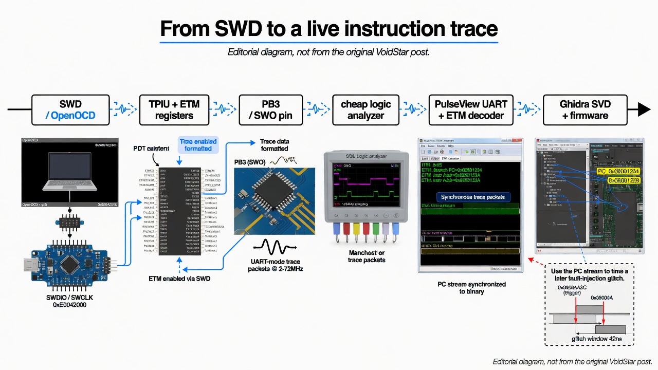
Overview
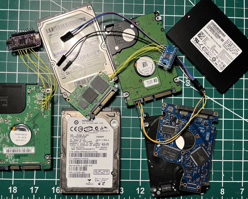
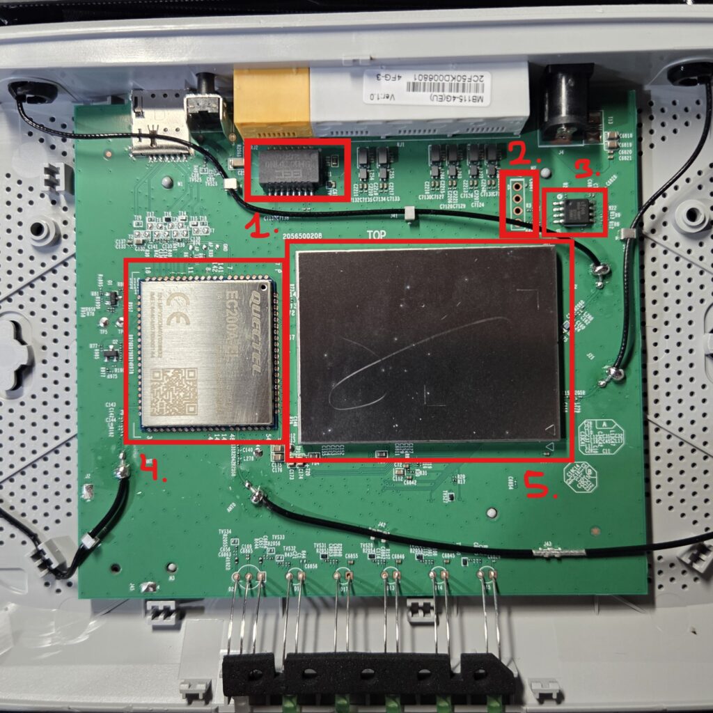
VoidStar’s earlier posts have spent a lot of ink on finding SWD and JTAG: the Xbox controller SWD teardown, brushing-up labs, PiFex JTAG, an SSD TAP. Those write-ups usually end at a dump. A live trace is the next layer of the same debug fabric. ARM CoreSight can stream a compressed, real-time record of execution. Firmware authors use it for runaway code, timing bugs, and performance. Reverse engineers get a cycle-accurate log of what the binary actually did, without planting breakpoints that change the race they are trying to watch.
Vendor boards with a proper SWO header and a vendor decoder make this look easy. An undocumented consumer gadget does not. Alt’s bet is that if the TPIU can be talked into UART-framed SWO, a $10 logic analyzer and Pulseview are enough. The target is the same STM32F401 Xbox One controller from the previous SWD post.
- Review the CoreSight trace components: the ETM, the ITM, and the TPIU
- Locate the single pin we need to physically tap on the target
- Configure the TPIU and ETM entirely from an OpenOCD config file
- Capture the resulting trace with a cheap logic analyzer and decode it in Pulseview
- Use Ghidra to diagnose (and eventually fix) why our trace keeps falling apart
Configs, scripts, and an example capture are in the etm-examples repository.
Goals
- Explain what the ETM, ITM, TPIU, and DWT each do and how they fit together
- Write an OpenOCD config file that enables instruction tracing on an STM32
- Capture Serial Wire Output (SWO) trace data with a logic analyzer instead of an expensive trace probe
- Recognize when your trace has desynchronized or is generating garbled output
Target
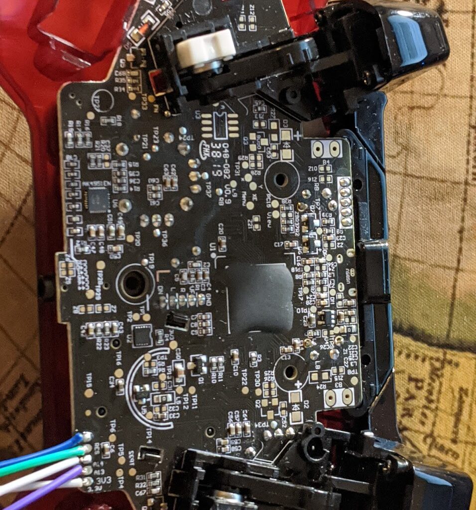
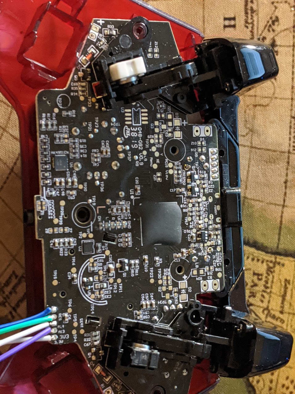
Long-time readers already know this board. It is a third-party Xbox One controller. The earlier post found a debug port, used OpenOCD to identify an unmarked MCU, and pulled firmware. This follow-up asks whether the same silicon will emit an instruction trace while the firmware runs. That is especially useful next to fault injection and differential power analysis — Alt flags a sequel for glitch timing, and this article does not invent that sequel.
The Trace Components: A Brief Tour
On-chip ARM debug and trace lives under the CoreSight name. The specification is public and large, split across at least three manuals that this post hops between constantly. Four blocks matter for a first capture.
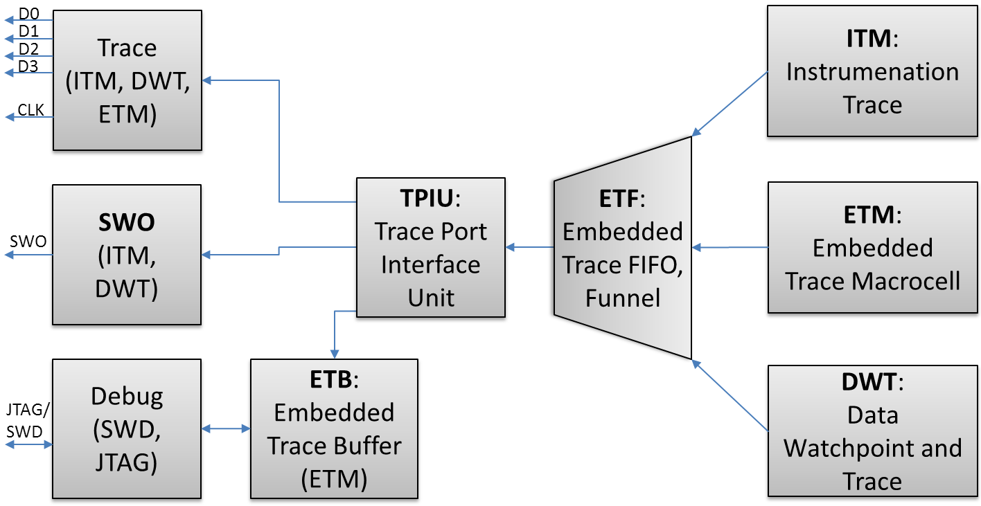
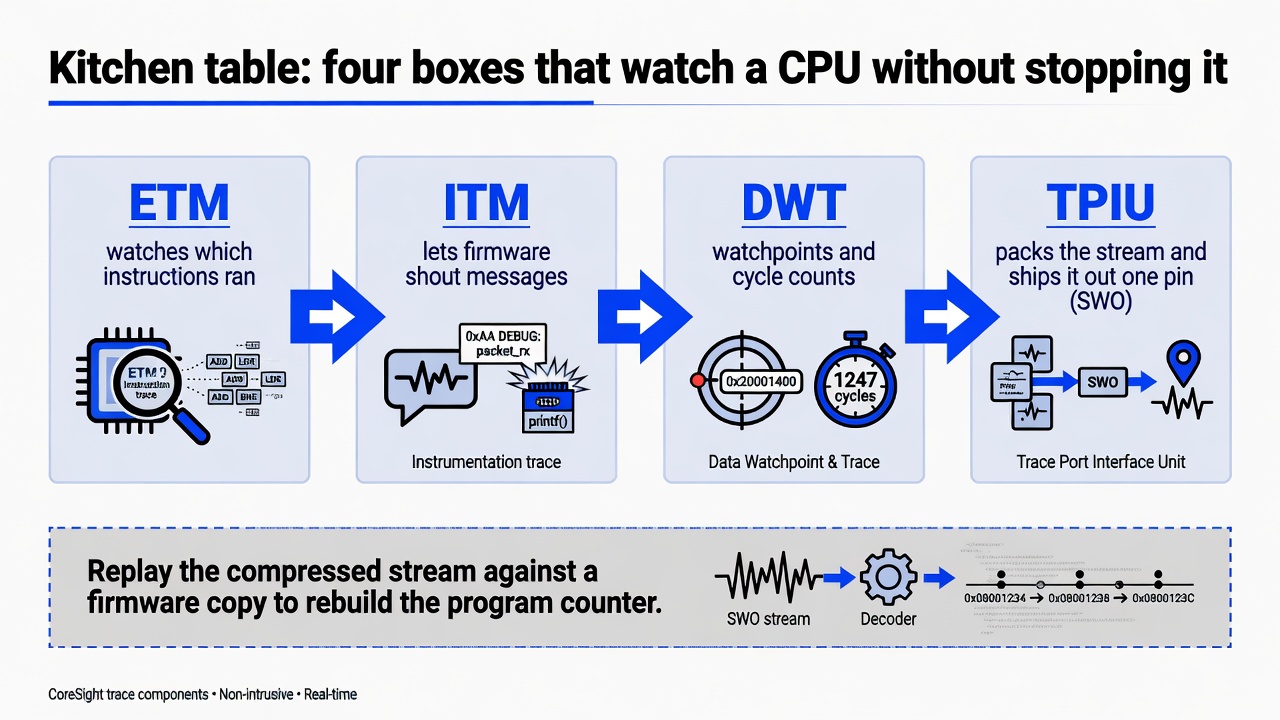
ETM (Embedded Trace Macrocell). The ETM watches execution and emits an instruction trace: a compressed stream of which instructions ran, whether branches were taken, and where the program counter went. It does not send every instruction byte. It sends the events a decoder cannot predict — branches, exceptions, periodic sync points. You reconstruct the path by replaying that stream against a copy of the firmware.
ITM (Instrumentation Trace Macrocell). The ITM is the software-driven cousin. Firmware pushes packets out the trace port. ARM SWO printf retargeting is ITM.
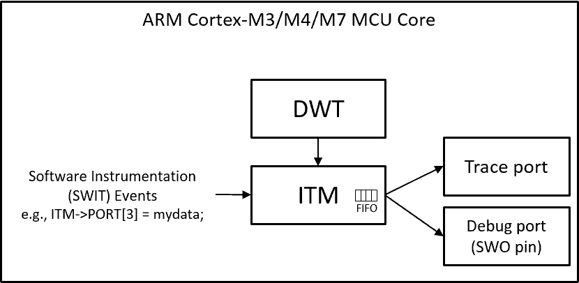
DWT (Data Watchpoint and Trace). Four comparators can watch a data address, an instruction address, a data value, or (comparator 0) a cycle count. The DWT raises debug events, can sample data, and sits next to ETM and ITM for data traces and profiling counters.
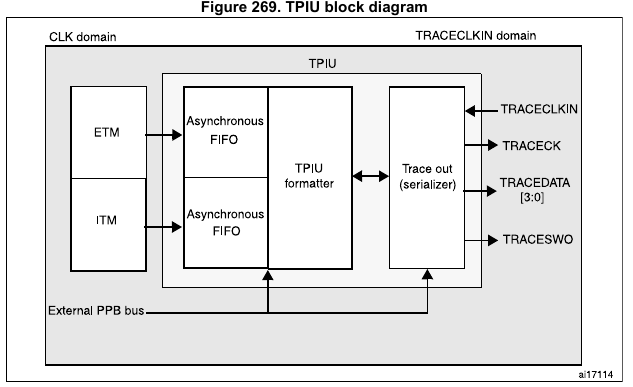
TPIU (Trace Port Interface Unit). Someone has to get the bytes off the die. The TPIU formats internal streams, optionally tags them with source IDs and timestamps, and drives a physical pin. That is the block a logic analyzer actually sees.
The ETM/ITM produce the data, the TPIU packages and outputs it, and we sit on the outside with a capture device trying to catch and decode it.
Matthew Alt, VoidStar Security
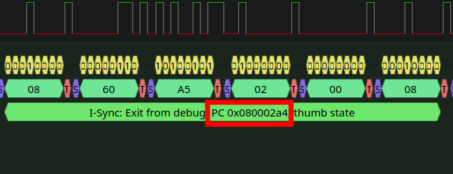
0x08000000. Trace ID (ETM_TRACEIDR) is stamped into TPIU frames; Alt uses ID 1. A decoder that locks onto the wrong ID, the wrong image, or the wrong Thumb bit will look “confidently wrong.” Always check the first PCs against the reset vector.Where does the data go? (Sinks)
Trace blocks can generate a lot of data. ARM defines several sinks:
- An Embedded Trace FIFO (ETF/ETB) — on-chip buffer you read back later
- A parallel Trace Port via the TPIU — fast, but needs a bunch of dedicated pins
- The Serial Wire Output (SWO) — a single pin, trace data shipped out asynchronously as UART-framed bytes
On this STM32F401 there is no on-chip trace buffer and no wide parallel port broken out, so SWO is the path. That is the whole accessibility trick. The “correct” capture box is an ARM ULINKPRO-D, a Lauterbach, or an IAR I-jet Trace. Because this part routes trace as async UART on one wire, a cheap analyzer and Pulseview will do.
The Target: Finding Our One Pin
Datasheet page 809 of stm32f401-ref.pdf lists the CoreSight lineup on this part: SWJ-DP, AHB-AP, ITM, FPB, DWT, TPIU, and ETM. When the TPIU is in asynchronous SWO mode, trace comes out on PB3.
The CPU sits under epoxy. PB3 is not silkscreened with a friendly arrow. After removing the MCU and the epoxy, a multimeter showed PB3 tied to R15.
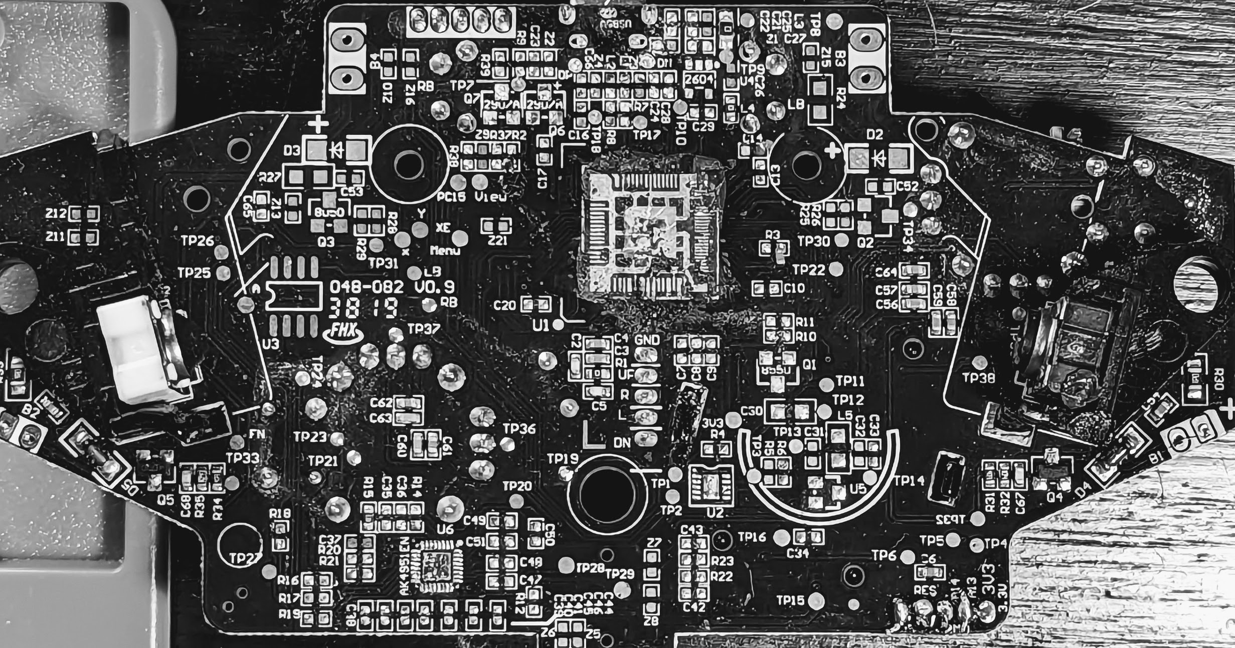
RE tip from the source: a working debug interface is a pin-hunting tool. Toggle a GPIO from OpenOCD and probe with a scope or analyzer. You typically need a datasheet to know which registers to poke; here they had one.
| Step | Status |
|---|---|
| Locate the PB3 pin | Connected to R15 |
| Configure and enable the TPIU | ??? |
| Configure and enable the ETM | ??? |
| Capture and decode data on PB3 | ??? |
Configuring the TPIU
The TPIU is configured first because it is the output path. The verbal contract Alt wants is: take whatever the ETM hands you, frame it, and shove it out SWO as 4 Mbaud async serial. The knobs are memory-mapped registers, written with OpenOCD mww. They live in the STM32F401 reference manual (document A) and the ARMv7-M Architecture Reference Manual (document B).
| Register | Address | Purpose |
|---|---|---|
DBGMCU_CR | 0xe0042004 | Debug MCU config – assigns the TRACE I/O pins |
COREDEBUG_DEMCR | 0xe000edfc | Sets TRCENA to power up the trace subsystem |
TPIU_CPSR | 0xe0040004 | Current Port Size Register |
TPIU_ACPR | 0xe0040010 | Async Clock Prescaler – this sets our baud rate |
TPIU_SPPR | 0xe00400f0 | Selected Pin Protocol – sync vs. async (UART) |
TPIU_FFCR | 0xe0040304 | Formatter and Flush Control |
Page 837 of document A gives a recommended power-on sequence. First the addresses as Tcl variables:
# Debug MCU configuration register
set DBGMCU_CR            0xe0042004
# Debug Exception and Monitor Control Register
set COREDEBUG_DEMCR     0xe000edfc
# TPIU Current Port Size Selection Register
set TPIU_CPSR           0xe0040004
# TPIU Asynchronous Clock Prescaler Register
set TPIU_ACPR           0xe0040010
# TPIU Selected Pin Protocol Register
set TPIU_SPPR           0xe00400f0
# Formatter and flush control register
set TPIU_FFCR           0xe0040304
Then the writes. setbits is a read-modify-write helper in the example config; mww overwrites the whole word:
init
reset halt
# TRACE_IOEN = 1, TRACE_MODE = 0 -> asynchronous tracing on TRACESWO
setbits $DBGMCU_CR 0x20                 ;# Enable the trace IO pins
# Set TRCENA in DEMCR to enable access to the trace registers
setbits $COREDEBUG_DEMCR 0x1000000
# Current port size
mww $TPIU_CPSR 1
# Async clock prescaler: trace clock = HCLK / (x + 1)
mww $TPIU_ACPR 3
# Pin protocol: 0 = sync, 1 = NRZ, 2 = USART/async
mww $TPIU_SPPR 2
# Formatter and flush control: 0x102 enables TPIU framing
mww $TPIU_FFCR 0x102
Source: original article. Two writes ate hours of debugging. TPIU_SPPR = 2 selects async UART-style protocol, which is why a UART decoder under ETM works. TPIU_ACPR is a divider: baud = HCLK / (ACPR + 1). Default 16 MHz HCLK and ACPR 3 yields 16 MHz / 4 = 4 Mbaud. The trace clock is derived from the core clock. If firmware later raises the PLL, the carefully chosen baud is suddenly wrong.
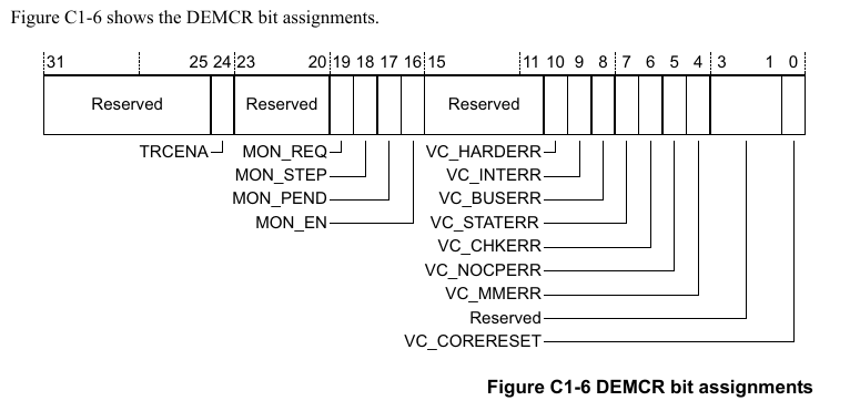
DBGMCU_CR bit TRACE_IOEN (0x20) plus TRACE_MODE = 0 is async TRACESWO. DEMCR.TRCENA (bit 24, 0x01000000) gates the whole trace subsystem; without it the TPIU/ETM windows ignore you. TPIU_FFCR = 0x102 turns on formatter framing so the decoder can recover source IDs. SPPR 0 = sync parallel, 1 = Manchester, 2 = NRZ/UART — pick 2 for a cheap analyzer.Configuring the ETM
The ETM follows the same pattern, but it is locked. A magic value has to hit the lock-access register before configuration writes stick. Registers come from the STM32F401 manual and the ETM Architecture Specification.
| Register | Address | Purpose |
|---|---|---|
ETM_LAR | 0xe0041fb0 | Lock Access Register – unlock write access |
ETM_CR | 0xe0041000 | Main Control Register |
ETM_TRACEIDR | 0xe0041200 | Trace ID – the source ID stamped on our stream |
ETM_TER | 0xe0041008 | Trigger Event Register |
ETM_TEE | 0xe0041020 | Trace Enable Event Register |
ETM_TSSR | 0xe0041024 | Trace Start/Stop Register |
The unlock constant is the CoreSight password you will keep seeing: 0xC5ACCE55 (“CoreSight ACCESS”). Configuration sits between two writes to ETM_CR: the first sets the programming bit, the last clears it so tracing begins. Trace ID 1 is what the decoder must look for.
set ETM_LAR             0xe0041fb0
set ETM_CR              0xe0041000
set ETM_TRACEIDR        0xe0041200
set ETM_TSSR            0xe0041024
set ETM_TER             0xe0041008
set ETM_TEE             0xe0041020

# Unlock write access to the ETM
mww $ETM_LAR 0xC5ACCE55
# Configure the trace (programming bit set)
mww $ETM_CR 0x00201d0e
# Trace bus ID = 1
mww $ETM_TRACEIDR 1
# Trigger event
mww $ETM_TER 0x0000406F
# Trace enable event
mww $ETM_TEE 0x0000006F
# Trace start/stop - enable the trace
mww $ETM_TSSR 0x00000001
# Control register - end of configuration
mww $ETM_CR 0x0000191E
Source: original article. Exact bit fields in ETM_CR and ETM_TER live in the ETM Architecture Specification. Datasheet-recommended values are a fine first trace.
| Step | Status |
|---|---|
| Locate the PB3 pin | Connected to R15 |
| Configure and enable the TPIU | Done |
| Configure and enable the ETM | Done |
| Capture and decode data on PB3 | ??? |
0xC5ACCE55 is the combination ARM printed in the manual on purpose. After you unlock it, you tell it which jersey number (trace ID) to stamp on every packet, then you close the padlock’s programming bit so the diary starts writing. If you never unlock it, your OpenOCD writes vanish into a locked window and you will swear the chip is broken.Capturing the Trace in Pulseview
OpenOCD will program the peripherals. A probe is soldered to PB3 via R15. Pulseview already ships an ETM protocol decoder. It is a stacked decoder: a UART layer recovers bytes from the wire, then ETM interprets those bytes.
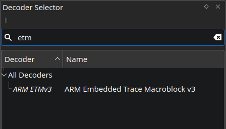
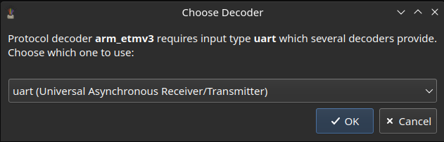
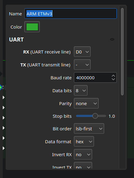
- UART decoder: RX on D0, baud rate
4000000 - Logic analyzer: 24 MHz sample rate, 25% pre-trigger capture ratio, falling-edge trigger on D0
A 4 Mbaud line wants several samples per bit; 24 MHz is six samples per bit. A falling-edge trigger starts on the first start bit; 25% pre-trigger keeps a little context. The workflow:
- Plug the controller into the Pi and run OpenOCD with the trace config (this programs ETM and TPIU)
- In the OpenOCD telnet console,
reset halt— ETM/TPIU config survives that reset - Arm the Pulseview capture
- Back in telnet,
resume
Data appears. Gaps, small bursts. The next question is whether it is ETM or garbage.
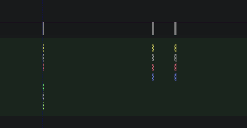
reset halt does not wipe the TPIU/ETM programming on this part — useful, and easy to forget when you assume DBGMCU is reset-sensitive.Reading the Trace (…initially)
A good trace is one where the decoder locks onto a synchronization point and then walks the program counter through addresses that exist in the image. At the start, that is exactly what happens: PCs march through the reset vector, then through a coherent early-startup path you can line up in Ghidra.

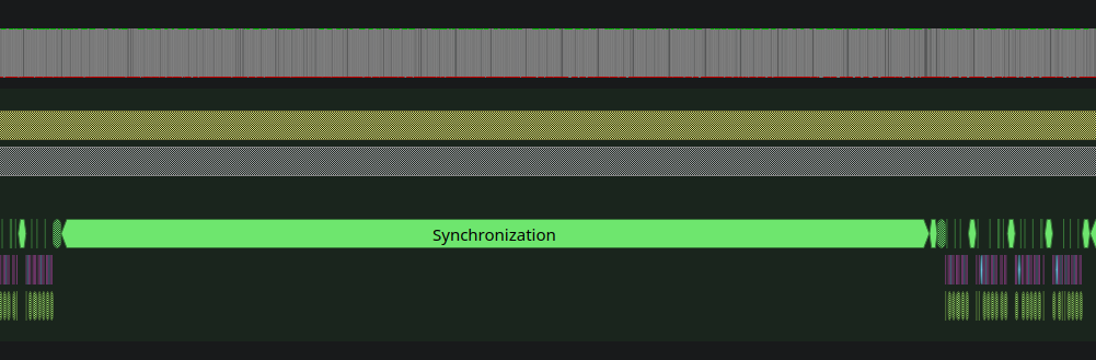
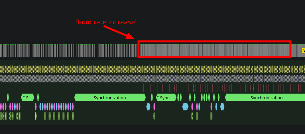
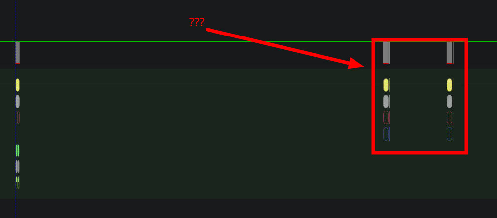
A little further in, a synchronization sequence appears in the middle of the stream. Immediately after it, the decoder emits garbage. The raw analog of the wire shows why: the baud rate increased mid-capture. The UART decoder is still locked at 4 Mbaud. Every recovered byte is wrong, so the ETM layer replays nonsense. Firmware reconfigured the clock; ACPR is a prescaler, not a fixed baud.
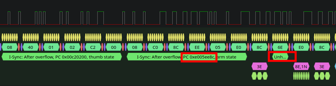
Two mysteries remain. Why does the clock change, and can it be stopped? What is the last thing the CPU does at the end of the usable trace? Pulseview cannot answer either. The firmware can.
Diagnosing With Ghidra
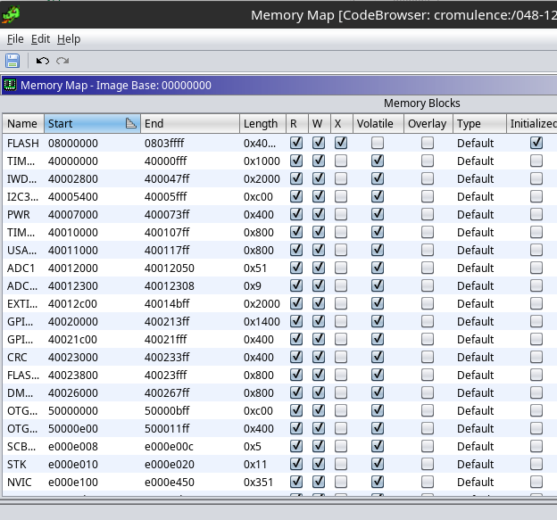
Cortex-M images are well documented: first word is the initial stack pointer, then the vector table, flash at 0x8000000 on this STM32. Load the dump as ARM Cortex little-endian at that base. Before auto-analysis, map peripherals. Without knowing that 0x40023800 is RCC, decompilation is a wall of offsets. Alt feeds Ghidra an SVD file with the SVD-Loader script and the STM32F401 SVD; the script builds the peripheral map and a struct per block.
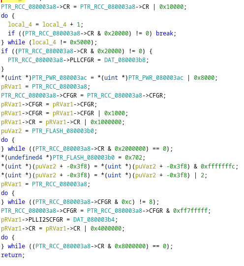
Retype a global as RCC* (Ctrl-L) and *(undefined4 *)(DAT_... + 0x08) becomes named register writes.
SVD-Loader is worth using on Cortex-M even when you are not tracing. SVD files ship in vendor CMSIS packs and on GitHub.
Mystery 1: The clock change
The last reliably decoded instruction sat around 0x8000390. That subroutine writes the RCC and the power controller to bring up the PLL:
pRVar2->PLLCFGR = DAT_1fff0fd4;
pRVar2->CFGR = pRVar2->CFGR & 0xffff03ff;
pRVar2->CFGR = pRVar2->CFGR | 0x800;
pRVar2->CR = pRVar2->CR | 0x1000000;
Source: original article, Ghidra decompilation. That is the core clock leaving the default 16 MHz. Because SWO baud is HCLK / (ACPR + 1), the wire speeds up with it.
Mystery 2: PB3 gets stolen
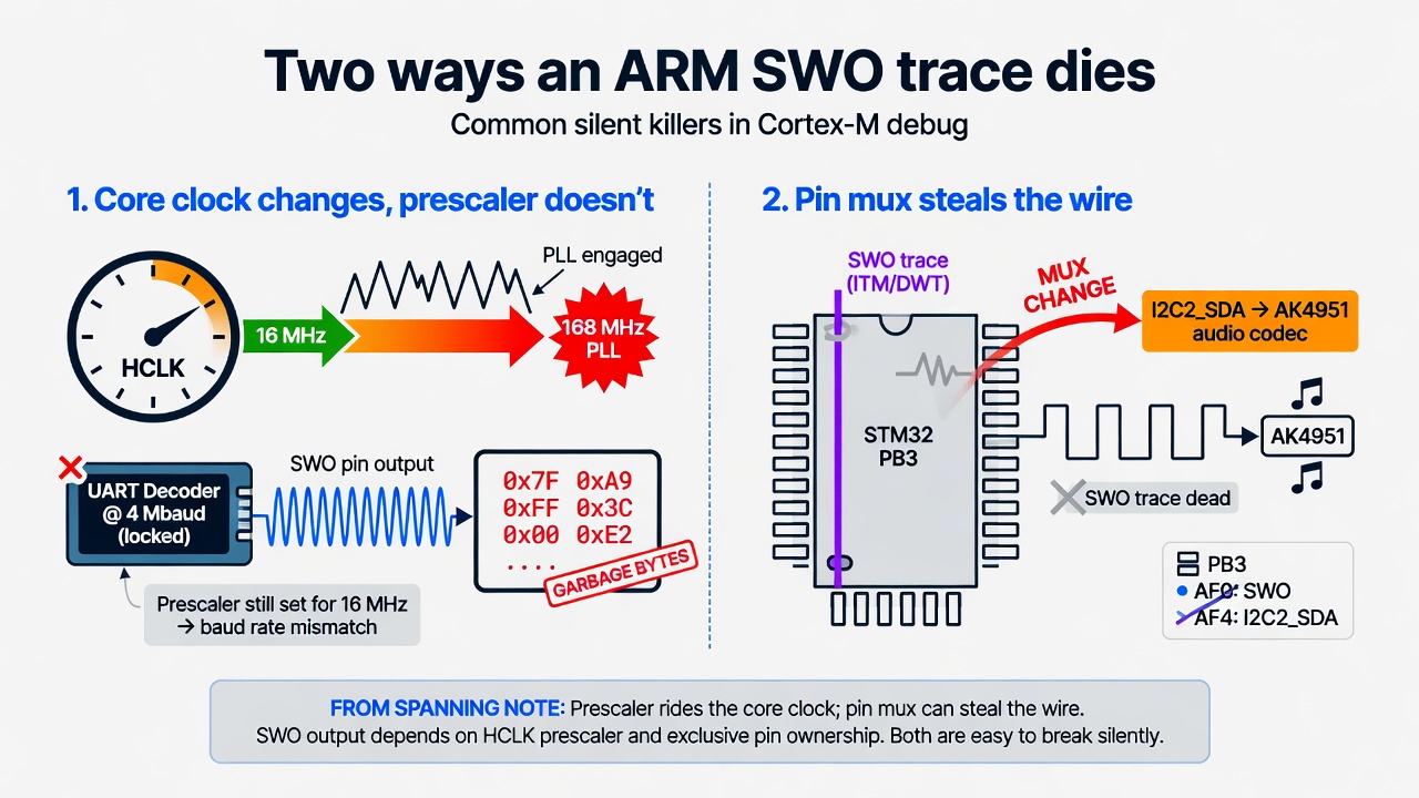
Zooming out in Pulseview after the baud change shows a second failure. PB3 stops looking like UART trace and starts looking like I2C. The STM32F4 alternate-function table says PB3 can be SWO or an I2C data line. On this controller the other end is an AK4951 stereo codec for headset audio. Startup reconfigures PB3 from SWO to I2C2 SDA. After that there is no trace on the wire to decode.

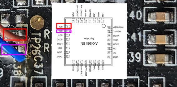
Two independent reasons the trace dies: PLL moves the baud, then firmware repurposes the pin. Clean traces need both problems handled.
Getting Better Traces
Clock first. If a longer readable stream exists after PLL bring-up, that stream can point at the instruction that reconfigures PB3.
Fix 1: Slow the trace clock back down
Firmware must configure its clock to function. The move is to raise TPIU_ACPR from 3 to 31 so that even a faster HCLK still lands in a baud the analyzer can follow. Timing still matters: set it before the PLL and the pre-PLL portion is unreadably slow; set it after and you already lost the transition. Let firmware finish clock setup, break right after, then reconfigure trace and go:
resume
reset halt
bp 0x80001fa 2 hw
resume
Source: original article. Hardware breakpoint on the instruction after the PLL routine returns (0x80001fa). Arm Pulseview, resume, capture from a settled clock. With ACPR 31 the stream is slow and steady. Breakpoints were finicky; two-byte Thumb hardware breakpoints (bp <addr> 2 hw) stuck best.
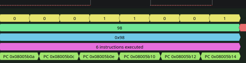
Fix 2: Stop the firmware from stealing PB3
A slower clock does not stop the I2C reassignment. Alt patches the image so those routines never run. Two functions matter. The first puts GPIOB pins into alternate-function I2C roles. With HAL structs imported, it is readable:
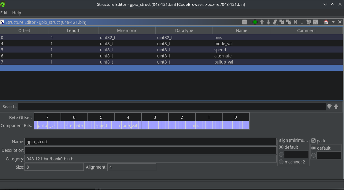
/* Pins 3 and 10 */
local_40.pins = 0b0000010000001000;
/* Mode = 2 (alternate function) */
local_40.mode_val = '\x02';
local_40.speed = '\x02';
local_40.alternate = '\x01';
local_40.pullup_val = '\0';
HAL_GPIO_Init((uint *)PTR_GPIOB_08005e04, &local_40);
/* Pin 4, AF10 -> I2C2_SCL */
HAL_GPIO_Set_AFRL((GPIOB *)PTR_GPIOB_08005e04, 10, 4);
/* Pin 3, AF9 -> I2C2_SDA  <-- there goes our trace pin */
HAL_GPIO_Set_AFRL((GPIOB *)PTR_GPIOB_08005e04, 3, 9);
Source: original article. The last call is PB3 → AF9 I2C2_SDA, which kills the trace. The second function brings I2C2 online:
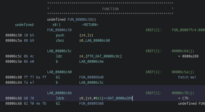
The fix in the post is blunt: overwrite the branches to those routines with ARM Thumb nop (0xBF00) and flash the modified image. PB3 stays SWO. Alt is explicit that this is a scalpel: headset audio is deliberately broken so a debug pin stays free. The result is not a fully functional controller.
The combined workflow
- Connect with OpenOCD (the config enables ETM and TPIU)
resumeto let the controller run its initial startupreset halt- Hardware breakpoint after PLL:
bp 0x80001fa 2 hw - Arm Pulseview — falling-edge trigger, 25% pre-capture
resume
With the patched firmware and the higher prescaler, the instruction trace survives well past where the original capture fell apart, and zoomed regions decode cleanly.

| Step | Status |
|---|---|
| Locate the PB3 pin | Connected to R15 |
| Configure and enable the TPIU | Done |
| Configure and enable the ETM | Done |
| Capture and decode data on PB3 | Done |
| Get long, clean traces | Done (via firmware patches) |
Bonus: Turning the Trace Pin On at Runtime
You will not always want to, or be able to, reflash. With SWD you can put PB3 back into SWO mode at runtime with memory writes. Alternate-function assignment lives in GPIOB at 0x40020400. Halt after firmware has stolen the pin, rewrite those registers toward a reset / SWO-compatible state, and the pin becomes trace again:
> mww phys 0x40020400 0x00000280
> mww phys 0x40020404 0x00000280
> mww phys 0x40020408 0x00000280
> mww phys 0x4002040C 0x00000280
> mww phys 0x40020410 0x00000280
> mww phys 0x40020414 0x00000280
> mww phys 0x4002041C 0x00000280
> mww phys 0x40020420 0x00000280
> mww phys 0xe0040010 15
Source: original article. The last write sets TPIU_ACPR to 15 for the current clock. Halt after bootloader/UART mode, fire the writes, tracing returns on SWO at roughly 4 MHz. A faster analyzer helps: a DSLogic at 100 MHz can follow a 20 MHz-class trace clock. The lab here used ~$15 FX2 analyzers.
This is the technique Alt says he uses more often for fault-injection research. A clean instruction trace next to a logic capture lines up the instant a specific instruction executes — the information you need to time a glitch. That rabbit hole is the promised next post. This article stops where he stops.
mww phys block as a universal STM32 script; the addresses are GPIOB on this F401 map.Why a garbled trace is still a finding
The useful engineering moral is not “buy a Lauterbach.” It is that a confident decoder is not ground truth. Alt’s first capture looked like ETM, then like sync, then like junk, then like I2C. Each of those appearances was a real event in silicon: PLL, then AF remap. If you only tune Pulseview you will spend a night on baud-rate superstition. If you open the image in Ghidra at the last good PC, the superstition turns into two functions with names.
The same moral applies when the capture is for offense. A glitch timed against a desynced trace is a glitch timed against fiction. Alt’s insistence on lining PCs up with the reset vector, then with Ghidra, is the quality bar. The cheap analyzer is allowed. The cheap interpretation is not.
| ATT&CK / lab note | How it shows up here |
|---|---|
| T1200 Hardware Additions | SWD probe plus a logic analyzer on PB3/R15 |
| T1601.1 Patch System Image (lab) | Thumb NOP 0xBF00 over I2C/GPIO init calls |
| T1059.008 Network Device CLI (cousin) | OpenOCD telnet: mww, setbits, bp, resume |
| Side channel for later T1495-class work | ETM PC stream as a glitch timing oracle (next post) |
| CWE-1244 Internal Asset Exposed | Production SWD/SWO left reachable under epoxy |
A lab notebook: clocks, locks, and what a PC stream is actually for
Three arithmetic facts carry almost all of the pain in this write-up. Write them on the analyzer lid. First: SWO baud is not a UART setting you picked in a menu. It is HCLK / (TPIU_ACPR + 1). Second: the ETM does not send instructions. It sends a delta stream that is meaningless without the same bytes Ghidra is looking at. Third: PB3 is a ball with a day job. On reset it can be SWO. Ten milliseconds later it can be someone else’s I2C. Every failed capture in the original post is one of those three facts arriving as a surprise.
| HCLK | ACPR | SWO baud | Notes |
|---|---|---|---|
| 16 MHz (reset default) | 3 | 4.0 Mbaud | First capture; UART decoder locked here |
| 16 MHz | 31 | 500 kbaud | Pre-PLL with the “slow” prescaler; sluggish but readable |
| higher PLL HCLK | 3 | HCLK/4 | First failure: decoder still at 4 Mbaud |
| higher PLL HCLK | 31 | HCLK/32 | Fix 1: stay inside the analyzer’s comfort zone |
| current clock after steal | 15 | HCLK/16 | Runtime recovery write in the bonus section |
Sample-rate arithmetic is the twin of baud arithmetic. Alt samples at 24 MHz for a 4 Mbaud line (six samples per bit) and mentions a DSLogic at 100 MHz when the trace clock climbs toward 20 MHz-class. A cheap FX2 that tops out near 24 MHz cannot follow a 20 MHz SWO no matter how clever Pulseview is. That is why Fix 1 exists: you are not only being kind to the UART decoder, you are staying inside the analog bandwidth of a $15 pod. If you have the faster pod, you can leave ACPR lower and keep time resolution for glitch work. If you do not, you buy time with division.
The CoreSight lock is a fourth fact that only hurts once, and then you never forget it. 0xC5ACCE55 is not a secret. It is a deliberate constant so that stray bus writes do not reprogram a live ETM. If your mww sequence skips the LAR, the control registers read back as if they accepted the values and then do nothing. That failure mode looks like a dead pin, a wrong AF, or a Pulseview bug. It is none of those. Always read ETM_CR back after the programming bit clears, and always confirm DEMCR.TRCENA is actually set. Alt’s scripts do the writes in the datasheet order; copy that order before you invent a shorter one.
Once the stream is honest, what is it for? The original post names the near-term uses without walking into the sequel: runaway-code hunting, timing bugs, performance, and lining a program-counter timestamp up with a power or reset line so a later glitch has an instruction to aim at. For firmware RE the everyday win is smaller and still huge. You watch the reset vector, you watch the PLL, you watch the first peripheral inits, and you get a ground-truth order of operations that static Ghidra can only guess. Functions that never run do not appear. Functions that run twice appear twice. The compressed trace is a dynamic cross-ref.
ETM_TRACEIDR (1 in the listing); (3) Thumb bit on Cortex-M is not optional — a decoder in ARM mode will look “almost right” and be wrong; (4) after any RCC write, re-measure bit time on the analog trace before you trust the UART layer; (5) if the line goes to 8-bit addresses with ACKs, stop, it is I2C. OpenOCD reset halt on this STM32 keeps TPIU/ETM programming, which is a gift. Do not assume that on the next vendor.Related VoidStar hardware notes that this post sits on, without duplicating them: the Xbox SWD teardown that identified the unmarked STM32F401, plus the JTAG/SWD series linked from the overview (brushing-up, PiFex, SSD TAP). Those are how you get the debug pipe. This post is what you do with the pipe once it speaks. The etm-examples repo is the companion for configs and a sample capture. Clone it for the Tcl; do not treat a random fork as a glitch framework.
One more operator caution about the published runtime GPIOB writes. They are a live mux patch for this F401 map, demonstrated after the firmware has already stolen PB3. They are not a generic “enable SWO on any STM32” one-liner. GPIOB base 0x40020400, the 0x280 pattern, and ACPR 15 are all specific to the story above. If you copy them onto a different family you can remap the wrong pins, including the SWD pair itself. Halt, read the AFR registers, compare to the datasheet AF table, then write. The original listing stays verbatim so you can see exactly what Alt typed; the caution is about where you type it next.
Key Takeaways
- ARM CoreSight can emit a live instruction trace without halting the core; ETM produces it, TPIU ships it, ITM/DWT ride along.
- On STM32F401, async SWO is one pin (PB3). A UART-stacked ETM decoder in Pulseview plus a cheap analyzer is enough if the TPIU is in NRZ mode.
- Baud is
HCLK / (ACPR + 1), not a constant. PLL bring-up will desync a decoder that assumed the reset clock. - The same pin can be stolen by pin mux. Here PB3 becomes I2C2 SDA to an AK4951. Decoder settings cannot fix a wire that is no longer SWO.
- Ghidra plus an SVD file turns the last good PC into named RCC and GPIO writes. That is how both failures were diagnosed.
- A higher ACPR, a hardware breakpoint after PLL, and (optionally) NOP patches or runtime GPIOB writes recover a long coherent trace.
- Configs and an example capture are in
etm-examples. A garbled stream that looks confident is still garbled until it matches the image.
Defensive Recommendations
- Treat SWD/SWO as an attack surface. If a consumer STM32 still enumerates SWJ-DP after epoxy, an instruction trace is a few register writes away. Disable debug in production (RDP, DBGMCU, TRACE_IOEN), and do not route SWO to a test pad you will ship.
- Epoxy is not a control. Alt removed a blob and still found PB3 at R15. Mechanical covering delays; it does not bind the TPIU.
- Pin mux is a control you can use. Reusing the SWO ball as I2C after boot accidentally killed the trace. Doing that on purpose, then locking the GPIO, shrinks the window where SWO is live.
- Clock trees leak. Anyone capturing SWO can see PLL bring-up as a baud step. That is a timing landmark for glitching. Avoid leaving TRACE enabled across that landmark on production units.
- Lab hygiene. Patched images that NOP audio init are not production firmware. Label them, keep them off the device that leaves the bench, and restore stock before any functional test you care about.
- Detection for device vendors. Unexpected
TRCENA,TRACE_IOEN, or ETM programming in a field dump is a sign someone is tracing. Include those registers in integrity snapshots. - For authorized RE. Always replay traces against the image. If PCs leave mapped flash, assume desync or the wrong Thumb mode before you assume exotic execution.
- Do not confuse a GitHub helper repo with a glitch kit. Use
etm-examplesas config and capture samples. The fault-injection sequel is a different post.
Conclusion
The post starts at “ARM cores have mysterious trace peripherals” and ends with a decoded instruction trace pulled off a running Xbox controller with a hobbyist analyzer. In between: three reference manuals, an OpenOCD file, a UART-stacked Pulseview decoder, a PLL that moved the baud, a codec that stole the pin, SVD-assisted Ghidra, a harsher prescaler, and a pair of NOPs. Peripheral configuration is the easy half once a datasheet exists. The hard half is the clock tree and the pin mux, and the willingness to open the firmware when the trace lies. The stream will happily hand you garbage and look confident doing it. Decode it against ground truth every time. Next, Alt wants that clean ETM stream sitting next to a synchronized logic capture so a glitch can be aimed at a single instruction. Until that post, the practical win is already on the table: after JTAG or SWD comes up, you are not done. You can watch the core run.
Questions, corrections, and cleaner OpenOCD recipes are invited in the original; the trace docs are famously thin. Hardware-RE roadmap, bootcamp, and debugger course links live on voidstarsec.com/roadmap. Thanks for reading — and happy hacking, from Matt.
Original text: “Following the Instructions: Live ARM Tracing with the ETM, ITM, and TPIU” by Matthew Alt at VoidStar Security Blog.