
Executive Summary
Xiaomi’s proprietary MJA1 secure chip appears in a growing range of the company’s IoT cameras but has never been publicly documented. Researchers at Quarkslab set out to change that through pure black-box analysis: no vendor documentation, no prior reverse-engineering work beyond a single photograph. Starting from bare hardware, they identified the chip’s I²C communication interface, dumped the NAND flash from two target devices, reverse engineered the host-side miio_client binary running on MIPS Linux, fully reconstructed the command protocol including its CRC-16/X-25 checksum variant, and then brute-forced all 256 possible command identifiers to discover two commands absent from the production firmware.
The protocol-level findings are reassuring: certificates and product data are immutable from the host side, private ECC keys never traverse the I²C bus, and the chip correctly rejects malformed inputs. Two undocumented commands were surfaced — an Update command (0x06) that can only write to an unprivileged user-data zone, and a mysterious command (0x13) that returns an undocumented error code. The deeper security questions — whether fault injection can bypass zone access controls, whether ECC side channels can leak private keys — remain open and are laid out as the natural next research phase. This post covers every step of the methodology in full technical detail.
Discovery of MJA1 Secure Chip
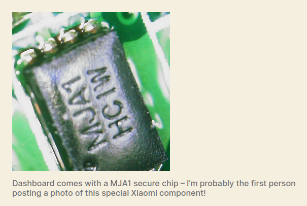
Xiaomi sells the MJA1 as a “hardware-level protection” component for device communications and sensitive data storage. Its marketing copy claims resistance to replay attacks, man-in-the-middle attacks, and brute force. Yet the chip is entirely proprietary: no datasheet, no SDK, no application notes in any public index. Before this research the only publicly available reference was a single photograph published by RoboCoffee in a February 2023 write-up on Brightway scooters.

The research goal was straightforward: determine how the chip works and evaluate its security properties from the outside. Nothing would be assumed; everything would be measured.
Target Identification
The team applied three selection criteria when choosing test hardware: the device must integrate an MJA1 chip, it must be affordable (under €50–100), and it must allow firmware upgrade traffic to be intercepted. Two devices met all three criteria:
- Xiaomi Outdoor Camera BW300 — approximately €60
- Xiaomi Camera Base Station — approximately €30
Both integrate the same MJA1 variant and can communicate with one another, enabling comparative analysis across two distinct PCB layouts. Having two devices with the same chip also provided a natural cross-validation path at every step.
Hardware Analysis
MJA1 Secure Chip Identification
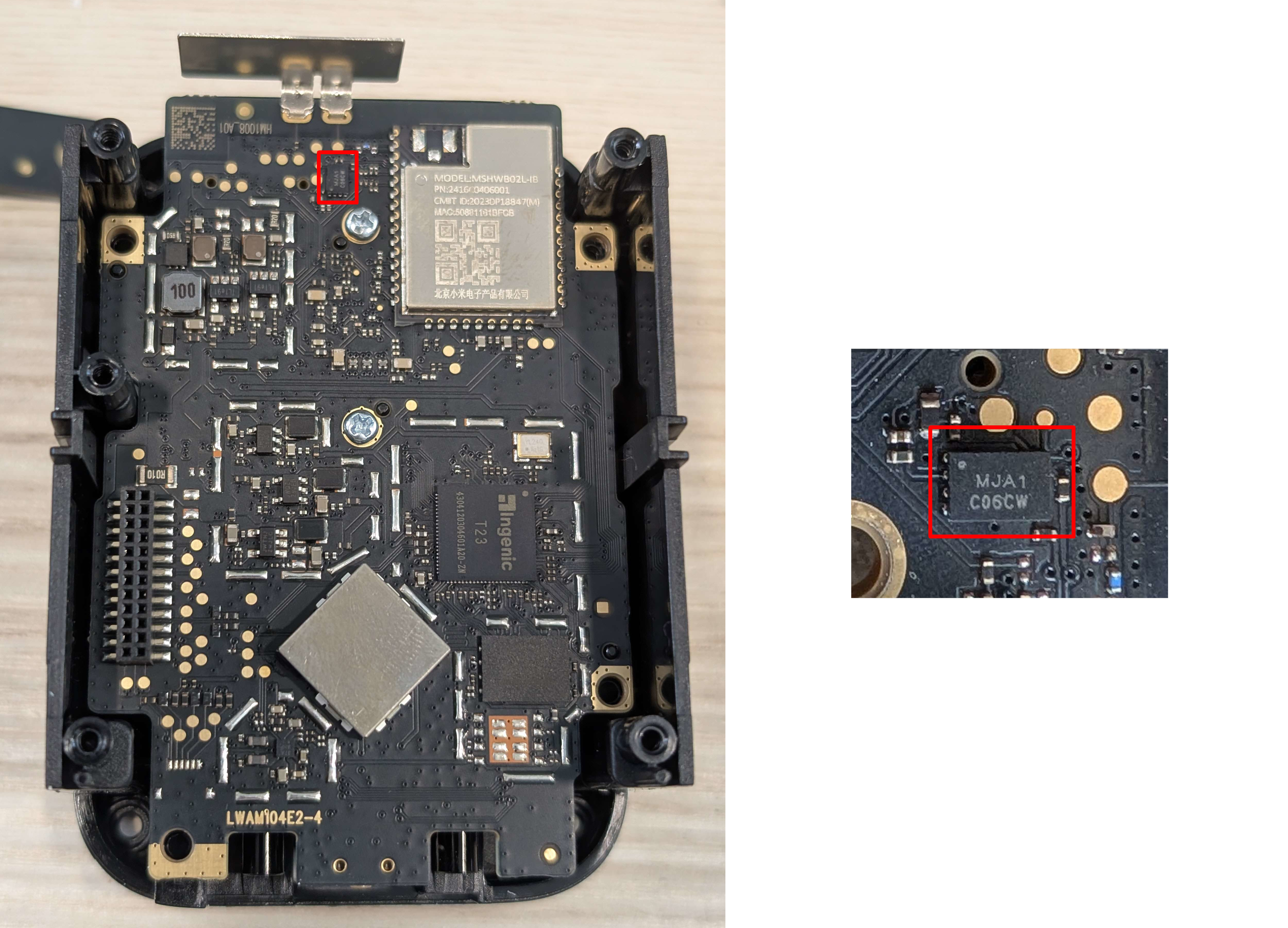
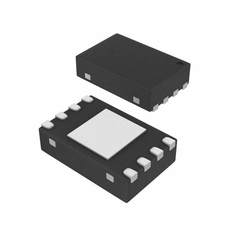
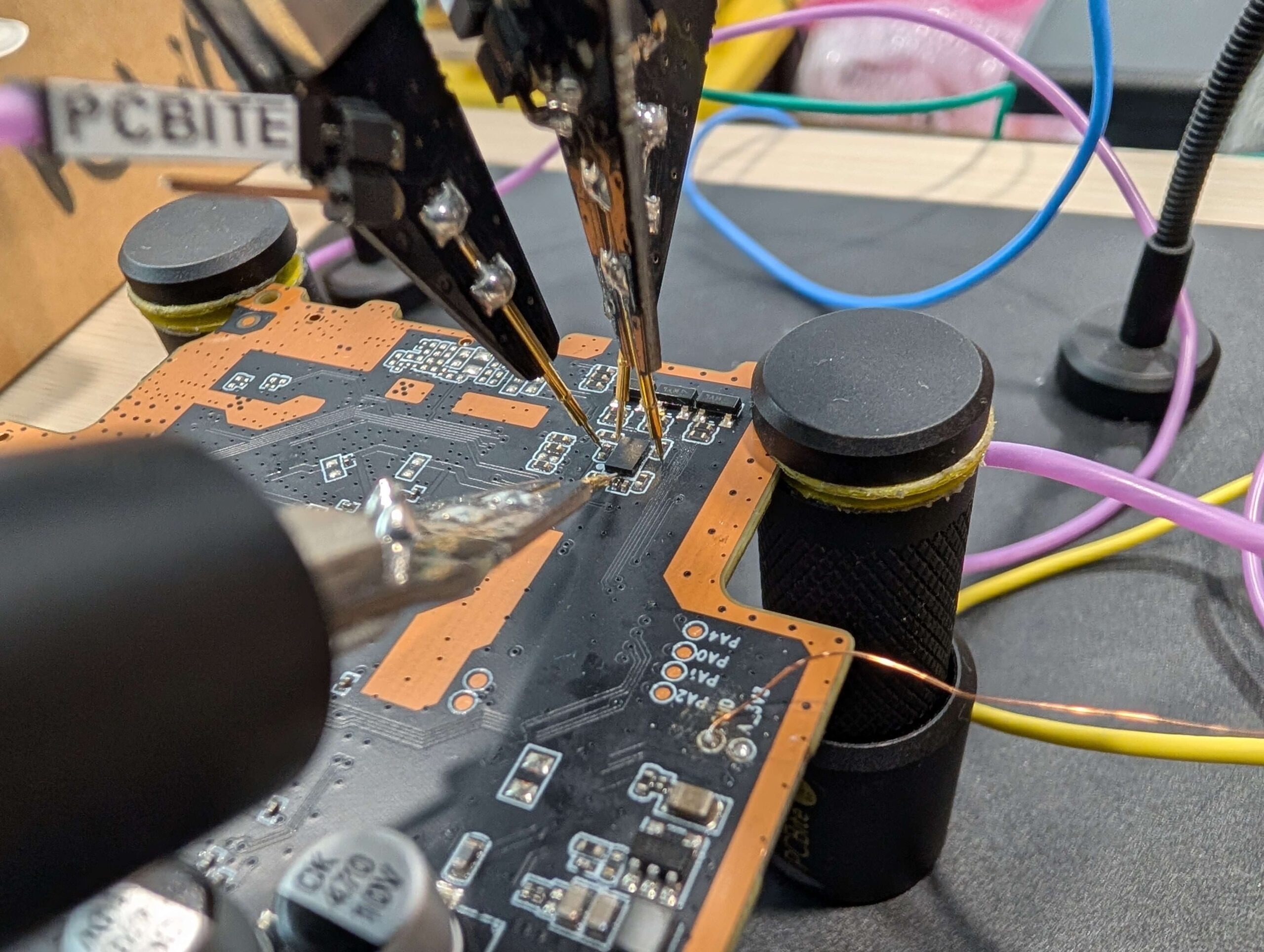
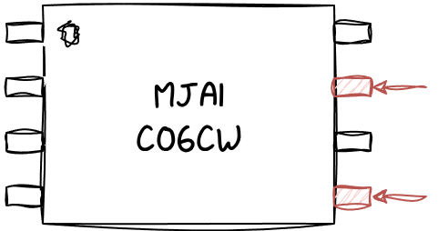
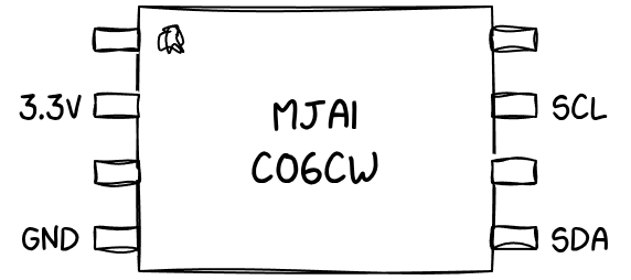
Opening both devices revealed the MJA1 on each PCB. The specific variant present in both is the MJA1 C06CW, housed in a DFN 2×3-8 package — a leadless Dual Flat No-lead form factor measuring 2 × 3 mm with eight pins on a 0.5 mm pitch. The DFN package made pin access non-trivial: probes had to be positioned precisely under live operating conditions to observe real traffic.
Sniffing Communications
A PCBite setup with a logic analyzer was positioned over the chip with all eight pins probed simultaneously while the Camera Base Station powered up and ran normally. Most pins held constant voltage levels (VCC pull-ups or GND), consistent with power, ground, and unused control lines. Only two pins showed dynamic transitions — periodic bursts of digital activity that clearly encoded data.
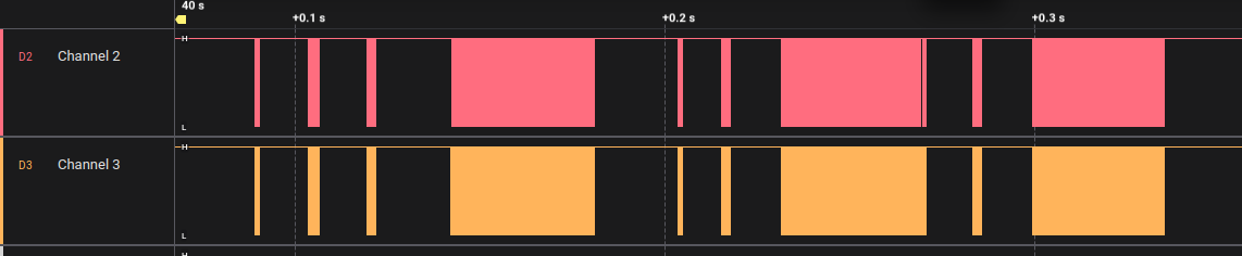
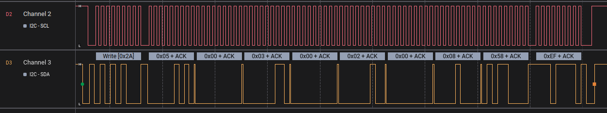
Zooming in on the two active signals made the protocol immediately recognizable. The waveform showed a distinct start condition, a regular square-wave clock line, and a data line whose bits are sampled on each clock edge — the unmistakable signature of an I²C bus. A captured transaction showed the host issuing a Write to address 0x2A, followed by the byte sequence 0x05, 0x00, 0x03, 0x00, 0x02, 0x00, 0x08, 0x58, 0xEF, each byte acknowledged by the chip. That sequence would later be decoded as a READ command once the protocol was fully reconstructed.
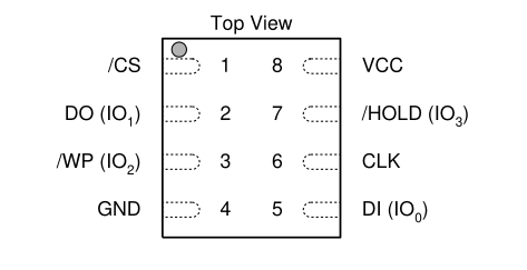
From this stage, the researchers established two facts: the communication protocol is I²C, and the MJA1 responds to the 7-bit address 0x2A. A full pinout diagram was then reconstructed from the probing data.
Flash Dumping
With the interface confirmed, the next step was obtaining firmware images from both devices to find host-side code that drives the MJA1.
Camera Base Station: The board carries an MD25Q128 SPI NOR flash chip supported directly by the TNM5000 universal programmer, so extraction was straightforward — attach, read, done.
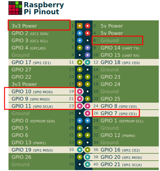
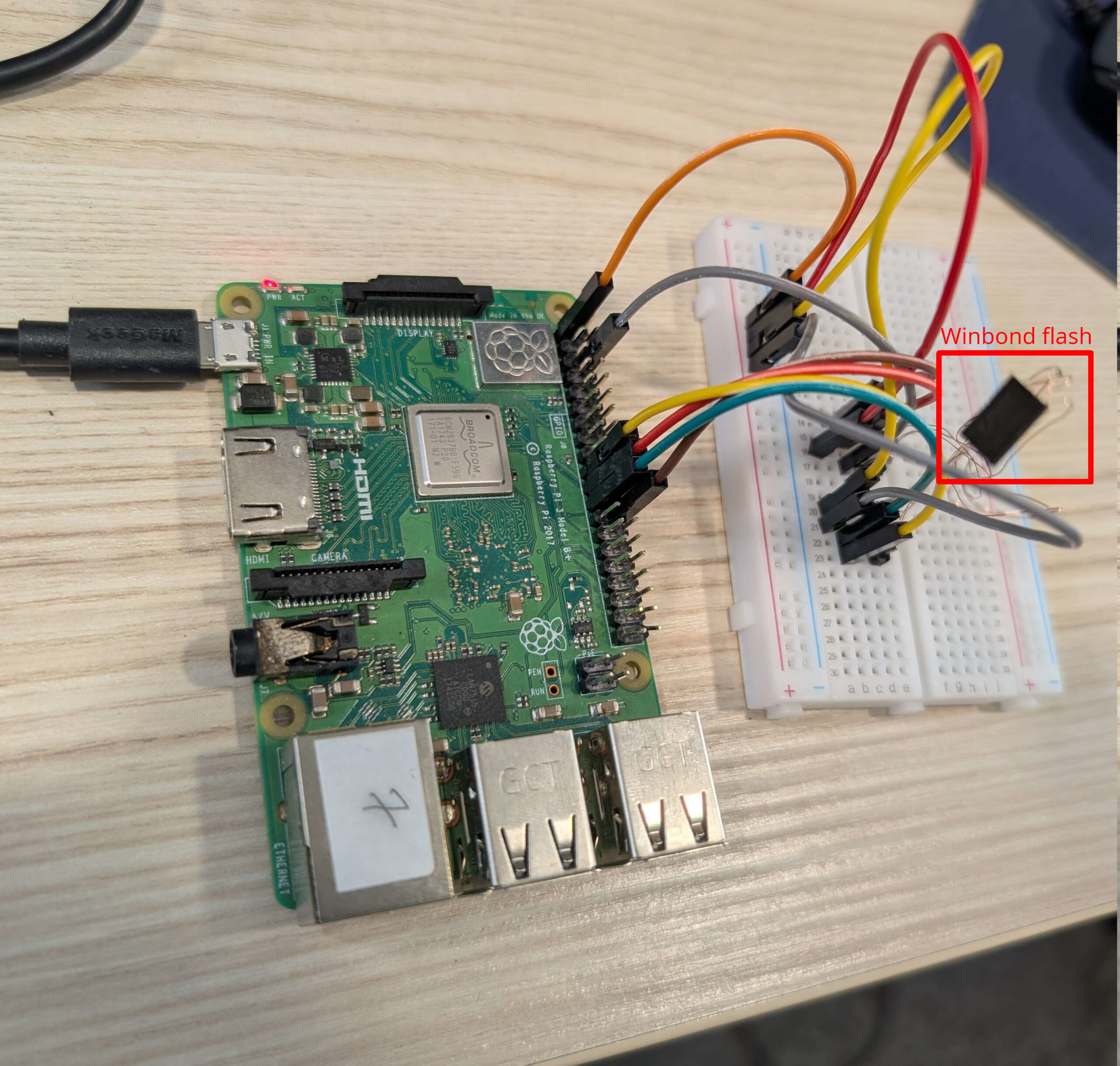
Xiaomi Outdoor Camera BW300: The camera uses a Winbond 25N01KVZEIR — a 1 Gbit SPI NAND flash in a WSON 8×6 mm package unsupported by the TNM5000. Instead, the team used a Raspberry Pi 3 B+ with its hardware SPI peripheral (SPI0) wired directly to the flash chip via a breadboard and Dupont cables.
| Winbond flash pin | Raspberry Pi pin |
|---|---|
| /CS | GPIO 7 (SPI0 CE1) |
| DO | GPIO 9 (SPI0 MISO) |
| /WP | 3.3V |
| GND | GND |
| DI | GPIO10 (SPI0 MOSI) |
| CLK | GPIO11 (SPI0 SCLK) |
| /HOLD | 3.3V |
| VCC | 3.3V |
The dump process was scripted in Python using the spidev module. First, the JEDEC ID was read to verify the wiring and SPI mode:
import spidev
import time

spi = spidev.SpiDev()
spi.open(0, 1)  # bus 0, device 1 (/dev/spidev0.1)
spi.max_speed_hz = 1000000
spi.mode = 0

# Send JEDEC ID read command (0x9F)
response = spi.xfer2([0x9F, 0, 0, 0, 0, 0, 0, 0])
print("JEDEC ID:", [hex(x) for x in response])
With the expected JEDEC ID confirmed (['0x0', '0x0', '0xef', '0xae', '0x21', '0x0', '0x0', '0x0']), the full 1 Gbit image was read page by page using the NAND page-load command (0x13) followed by a cache-read command (0x03):
import spidev
import time

# === Configuration ===
MAX_PAGE_NUMBER = 0x10000
PAGE_SIZE = 2048 # Size of data area (without spare/OOB)
SPI_BUS = 0
SPI_DEVICE = 1

# === Setup SPI ===
spi = spidev.SpiDev()
spi.open(SPI_BUS, SPI_DEVICE)
spi.max_speed_hz = 10_000_000
spi.mode = 0b00

# === Helper: Wait until NAND is ready ===
def wait_ready():
    while True:
        spi.xfer2([0x0F, 0xC0])        # 0x0F: Read status, 0xC0: Status register
        status = spi.readbytes(1)[0]
        if (status & 0x01) == 0:       # Bit 0 == 0 means "Ready"
            break
        time.sleep(0.001)

# === 1. Load page into cache using command 0x13 ===
def load_page_to_cache(page_number):
    addr = page_number.to_bytes(3, 'big')  # 24-bit address
    spi.xfer2([0x13] + list(addr))
    wait_ready()

# === 2. Read data from cache using 0x03 command ===
def read_cache_data():
    data = []
    for i in range(0, PAGE_SIZE, 4):
        addr = i.to_bytes(2, 'big')
        data += spi.xfer2([0x03] + list(addr) + [0x00, 0x00, 0x00, 0x00, 0x00])[4:]
    return data

with open("dump.bin", "wb") as f:
    for page in range(MAX_PAGE_NUMBER):
        print(f"Reading page {page}...")
        load_page_to_cache(page)
        page_data = read_cache_data()
        f.write(bytes(page_data))

spi.close()
Firmware Analysis
Reverse Engineering miio_client
Both firmware images were unpacked using binwalk and unblob, then the SquashFS partitions were mounted to access the root filesystem. The key binary was miio_client, which contained dozens of symbol names prefixed with mjac (MJA Chip) — functions like mjac_reset, mjac_get_did, mjac_get_certificate_pem, mjac_crc16_ccitt, and mjac_i2c. The symbol table was intact despite the section headers being stripped, making static analysis straightforward.
$ strings mi_ot/miio_client
...
mjac_reset
mjac_get_did
mjac_get_certificate_pem
mjac_crc16_ccitt
mjac_i2c
...
$ file mi_ot/miio_client
mi_ot/miio_client: ELF 32-bit LSB executable, MIPS, MIPS32 rel2 version 1 (SYSV), dynamically linked, interpreter /lib/ld-uClibc.so.0, no section headerThe binary is a 32-bit MIPS ELF for the uClibc toolchain — a common profile for Xiaomi’s embedded Linux camera platforms. Key functions identified through reverse engineering include:
mjac_init: initializes the I²C interface and establishes the connection to the chipmjac_cmd_build_<cmd>: a family of functions that construct properly formatted command frames for each supported operationmjac_resp_parse_data: parses the chip’s response frames and extracts the payloadmjac_crc16_ccitt: computes the frame integrity checksum
From the mjac_cmd_build_* functions, a complete table of supported commands was reconstructed:
| ID | Command | Category |
|---|---|---|
| 0x00 | Echo | Utility |
| 0x02 | Generate random | Utility |
| 0x05 | Read | Data access |
| 0x0D | Hibernate | Utility |
| 0x11 | Generate key | Cryptographic |
| 0x14 | Query | Data access |
| 0x16 | Generate signature | Cryptographic |
| 0x17 | Verify signature | Cryptographic |
| 0x18 | Establish key | Cryptographic |
mjac_cmd_build_* functions in miio_client. Source: original article.During research, the team also discovered github.com/iomonad/handshow-firmware, a public repository containing MJA1 wrapper source code (mjac_wrapper.c/h and mjac_defs.h). This served as an independent cross-validation of the command list and supplied additional details on argument layouts and response codes.
Command Format
The frame format was recovered by reverse engineering mjac_cmd_build_establish_key, which has a fixed-size payload and is easy to follow in decompiled form:
int mjac_cmd_build_establish_key
    (__mjac_cmd_establish_key *_cmd, uint _cmd_len, void *_src, int _src_len)
{
  ushort crc;
  int ret;

  if (_src == (void *)0x0) {
    return 0;
  }
  if (_src_len == 0x45) {
    if (_cmd == (__mjac_cmd_establish_key *)0x0) {
      ret = 0;
    }
    else {
      ret = 0;
      if (0x48 < _cmd_len) {
        _cmd->field0_0x0 = 0x18;
        _cmd->field1_0x1 = 0xff;
        memcpy(_cmd->___key,_src,0x45);
        crc = mjac_crc16_ccitt(&_cmd->field0_0x0,0x47);
        _cmd->_crc16_lo = (char)crc;
        _cmd->_crc16_hi = (char)(crc >> 8);
        ret = 0x49;
      }
    }
    return ret;
  }
  return 0;
}
The frame layout generalizes as follows: byte 0 is the command ID (here 0x18), byte 1 is a constant 0xFF whose purpose is unclear, bytes 2 through N carry the command-specific payload, and the final two bytes are the CRC-16 computed over all preceding bytes in little-endian order. The total frame for Establish key is 0x49 bytes.
Reverse engineering mjac_crc16_ccitt revealed that the checksum is CRC-16/X-25 (also known as CRC-16/IBM-SDLC), characterized by a reflected (LSB-first) implementation using polynomial 0x8408 (bit-reversal of 0x1021), initial value 0xFFFF, and a final bitwise inversion. A working C implementation derived from the decompiled lookup table:
static const uint16_t crc16_table[256] = {
    0x0000, 0x1189, 0x2312, 0x329B, 0x4624, 0x57AD, 0x6536, 0x74BF,
    0x8C48, 0x9DC1, 0xAF5A, 0xBED3, 0xCA6C, 0xDBE5, 0xE97E, 0xF8F7,
    /* ... 240 more entries (full table in original article) ... */
    0x7BC7, 0x6A4E, 0x58D5, 0x495C, 0x3DE3, 0x2C6A, 0x1EF1, 0x0F78,
};

uint16_t crc16(const uint8_t *data, int len) {
    uint16_t crc = 0xFFFF;
    for (uint32_t i = 0; i < len; i++) {
        crc = crc16_table[(crc ^ data[i]) & 0xFF] ^ (crc >> 8);
    }
    return ~crc;
}
The READ command (ID 0x05) was the first concrete example decoded from the original I²C capture. Its frame carries four fields after the command byte: an Index selecting the data zone, an Offset within that zone, a Length capped at 512 bytes, and the two-byte CRC. The five available data zones are:
| Index | Zone |
|---|---|
| 0 | Device certificate |
| 1 | Manufacturer certificate |
| 2 | Root certificate |
| 3 | Product data |
| 4 | User data |
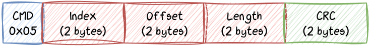
A concrete example: the captured I²C transaction 0x05, 0x00, 0x03, 0x00, 0x02, 0x00, 0x08, 0x58, 0xEF decodes as READ(Index=3, Offset=2, Length=8, CRC=0x58EF) — a read of 8 bytes from the product data zone at offset 2. The chip’s response was [00 | 000A | 00 00 00 00 41 FF E5 6F | 71C8]: status OK, length 0x000A, product ID 0x41FFE56F, CRC 0x71C8.
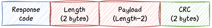
All responses share the same envelope: a status byte, a 16-bit length field, the response payload, and a trailing CRC-16. The defined status codes are:
| Code | Meaning |
|---|---|
| 0x00 | OK |
| 0x01 | Invalid CRC |
| 0x02 | Invalid arguments |
| 0x04 | Unsupported command |
| 0x06 | Length too large |
An important security observation: the three certificate zones (indices 0–2) are publicly readable and contain the device’s certificate chain. Private key material is never returned by any read operation; it remains internal and is only consumed by the cryptographic commands (Generate key, Generate signature, Establish key).
Testing
Testing Setup
Active command testing was performed on a rooted Xiaomi Camera C301, which also carries an MJA1 chip and runs Linux with a standard /dev/i2c-0 device node. A purpose-built C program provided the I²C interface:
int fd = open("/dev/i2c-0", O_RDWR);
ioctl(fd, I2C_SLAVE, 0x2A);
write(fd, cmd, cmd_len);
read(fd, resp, resp_len);
A dispatch table mapped command names to builder functions, enabling interactive invocation from the command line:
$ ./mjac_send read 3 2 8        # READ zone=3, offset=2, length=8
$ ./mjac_send query             # query chip info
$ ./mjac_send custom 130000...  # send arbitrary frame for fuzzing
A critical behavioral anomaly appeared immediately: after each command was sent, the chip became unresponsive and required a full device reboot before it would answer again. Extensive debugging and comparison against legitimate miio_client I²C traffic did not reveal the cause. One-at-a-time testing remained possible, making the brute-force approach viable at the cost of automation overhead.
Brute-Forcing Command IDs
With the full 256-byte command ID space to explore, the team automated the reboot cycle from a laptop over SSH. The controller script opened an SSH connection to the camera, ran the C test binary with the candidate command ID, captured and logged the response, rebooted the device via SSH if the chip went unresponsive, waited for the camera to come back online, then advanced to the next ID. Commands returning status 0x04 (Unsupported command) were classified as absent; all other responses were flagged for investigation.
After iterating through all 256 IDs, two previously unknown commands surfaced:
- 0x06 → Update: writes data to a zone
- 0x13 → Unknown: returns error code 0x0F, an undocumented status not listed in the firmware’s error table, suggesting the command exists but requires specific preconditions or arguments not yet identified
Update Command (0x06)
Despite its name, the Update command (0x06) is not a firmware update mechanism. Its frame structure mirrors the Read command exactly — same fields, same CRC — but writes data into a zone rather than reading from it.
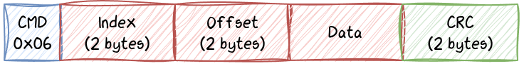
Access control is strictly enforced: only the user data zone (Index 4) accepts writes; all other zones return an error. Data length is bounded by the I²C buffer size, and the offset must fall within the user data zone bounds. The device certificate, manufacturer certificate, root certificate, and product data zones are all read-only from the host’s perspective — the chip refuses every write attempt targeting those zones.
Key Takeaways
- The MJA1 C06CW communicates over I²C at address 0x2A using the frame format: [Command ID | 0xFF | Payload | CRC-16/X-25]
- Nine commands are documented in production firmware; two additional commands (0x06 Update, 0x13 Unknown) were discovered through exhaustive brute-force of all 256 command IDs
- Private ECC key material never appears on the I²C bus; it is used exclusively by on-chip cryptographic operations (key generation, ECDH, signing)
- Write access is restricted to the user data zone (Index 4); all certificate and product data zones are immutable from the host side
- The chip correctly validates CRC integrity and rejects malformed arguments with appropriate error codes — no obvious protocol-level vulnerabilities
- Command 0x13 returns undocumented status 0x0F, hinting at hidden functionality or preconditions not yet understood
- Black-box methodology (I²C sniffing + firmware RE + brute-force) can fully reconstruct a proprietary secure element protocol using off-the-shelf tooling: a logic analyzer, a Raspberry Pi, and a disassembler
Defensive Recommendations
- Commission fault injection assessments: Protocol correctness does not imply physical tamper resistance — voltage glitching, EM pulses, and clock glitching against the chip itself remain untested; vendors should require these before claiming tamper resistance
- Apply constant-time ECC implementations: Generate key, Generate signature, and Establish key all perform ECC computations vulnerable to power and EM side-channel analysis; implementations should use constant-time algorithms and physical shielding
- Document the full command set publicly: Undocumented commands like 0x06 and 0x13 force integrators to reverse engineer what vendors should disclose; if 0x06 is write-restricted to the user zone, that guarantee should be documented and contractually binding
- Audit and disable provisioning commands in production: Command 0x13’s undocumented 0x0F status may indicate a debug or provisioning path; vendors should disable any non-production commands before shipping and verify this through security testing
- Treat I2C-accessible data as public: Certificate zones 0–2 are readable by any process with I²C access on a rooted device; applications must not rely on the confidentiality of data in those zones
- Harden the host OS against local privilege escalation: The chip’s access controls assume the host firmware behaves correctly; on embedded Linux devices where root is achievable, an attacker can issue arbitrary I²C commands, making OS-level hardening a prerequisite for relying on the secure element
- Use the chip’s ECDH and signature commands for firmware authentication: The MJA1 supports ECDH key agreement and ECC signatures; system designers should leverage these to authenticate firmware and OTA updates rather than relying solely on transport-layer protections
Conclusion
Starting from zero public documentation, Quarkslab researchers fully characterized the MJA1 C06CW’s communication interface, extracted firmware from two different Xiaomi camera platforms using both a universal programmer and a custom Raspberry Pi SPI rig, reverse engineered the host-side MIPS binary to reconstruct the complete command set and CRC algorithm, and brute-forced the entire command ID space to surface two previously unknown commands. The resulting protocol map — nine documented commands plus two discovered ones, five data zones with enforced write protection, private keys that never leave the chip — shows a design that behaves correctly at the protocol level. As the researchers note, the protocol work is the easy part; the more consequential questions about fault injection, side-channel leakage from ECC operations, and the behavior of the mysterious 0x13 command are only answerable once the chip is physically isolated and placed under direct analog scrutiny.
Original text: “Black Box Probing: a Security Analysis of Xiaomi’s MJA1 Secure Chip” by Mengsi Wu at Quarkslab Blog.